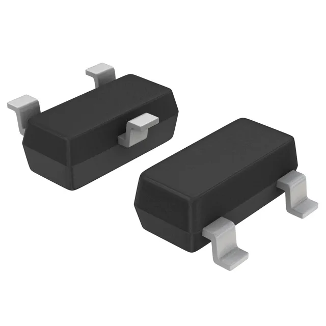
Gate drive and switching loss budget
Gate charge is 6.9 nC at 4.5 V, and input capacitance is 570 pF at 16 V drain. These numbers are low enough that a GPIO pin with a series resistor can drive the gate at moderate switching frequencies — no dedicated gate driver needed for sub-100 kHz PWM. The ±12 V Vgs maximum gives headroom if the gate is driven from a 12 V rail through a level shifter. The 1.3 W power dissipation at 25°C ambient is the thermal budget for the SOT-23 package. For a 4.3 A load, the conduction loss at 54 mOhm is about 1 W — that leaves only 0.3 W for switching losses before the junction hits 150°C. Derate the continuous current if the board copper area is small or ambient temperature exceeds 70°C.
Active production, no obsolescence worry
ROHS3 compliant. The SOT-23 package is a common industry footprint, so dual-sourcing from other manufacturers is straightforward if the BOM requires a second source.