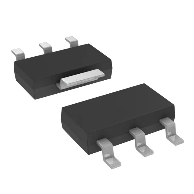
55 V, 5 A N-channel switch in SOT-223
It is housed in a surface-mount SOT-223 package with the drain tab as the primary thermal path.
Gate charge and drive voltage — switching budget
Input capacitance of 380 pF at 25 V drain-source confirms the gate drive load is light; a standard microcontroller GPIO with 10 mA source-sink capability charges the gate in under 40 ns.
Thermal and temperature range
Derate the 5 A continuous current rating above 25 °C case temperature — at 100 °C case temperature the allowable drain current drops to approximately 3.5 A, following the typical MOSFET derating curve.