Logic-level gate: one less driver on the BOM
The gate threshold voltage maxes out at 2.5 V at 250 µA, and the drive voltage range for achieving the rated Rds(on) spans 4.5 V to 10 V. That means a 5 V microcontroller output or a standard 5 V PWM signal can fully enhance the FET without a dedicated gate-driver IC — a real BOM simplification for low-voltage battery-powered systems or 5 V logic-controlled loads.
Gate charge and input capacitance — sizing the drive
Total gate charge is 140 nC at 4.5 V, and input capacitance (Ciss) measures 11210 pF at 50 V Vds. But the 140 nC charge also means the gate-drive source impedance must be low enough to avoid excessive switching losses during the Miller plateau; a 10 Ω to 22 Ω series gate resistor is a typical starting point for balancing rise time against ringing.
Thermal headroom in the TO-220AB
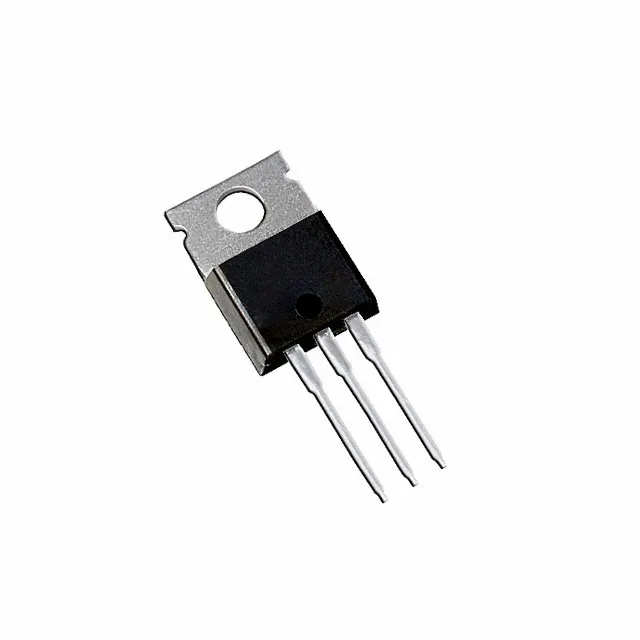
The 175°C Tj(max) is the upper limit for military and downhole applications — the same rating as many high-reliability parts. In practice, the 380 W ceiling is only reachable with an infinite heatsink; real-world designs derate based on the thermal resistance junction-to-case and the available heatsink area. The through-hole TO-220AB package allows a direct bolt-down to a chassis or heatsink, which is still the most thermally efficient mounting method for a discrete power FET.