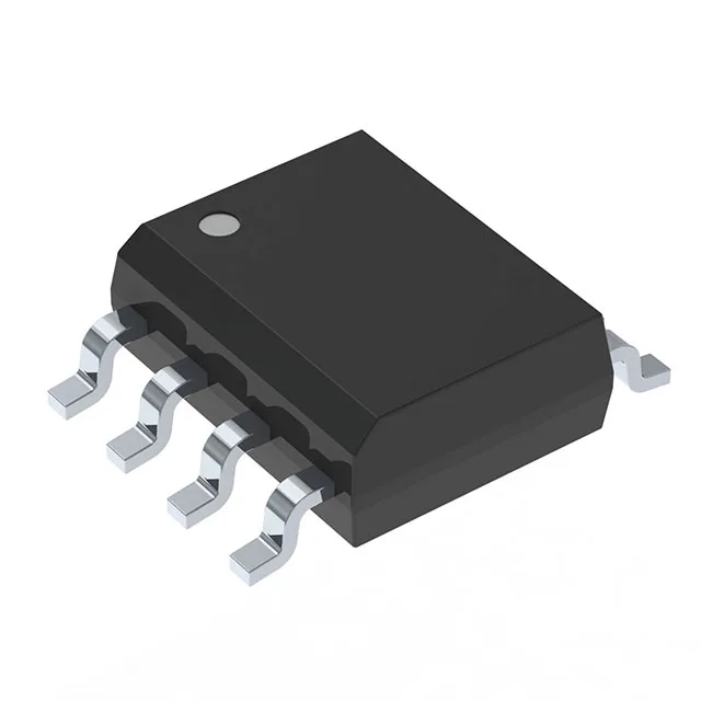
Infineon Technologies IRL6372TRPBF

IRL6372TRPBF HEXFET Dual N-Ch MOSFET, 30V 8.1A Logic Level

MPNIRL6372TRPBF
End of Life

Infineon HEXFET® IRL6372TRPBF, dual N-channel MOSFET, 30V Vdss, 8.1A Id, 17.9mOhm Rds(on) at 4.5V, logic-level gate, 8-SOIC package, -55°C to 150°C.

$0.9Ref. price · indicative, final on quote
Packaging8-SOIC (0.154", 3.90mm Width)
StockContact for availability
MOQ1 pcs
  • 100% new & originalTraceable channels only — no refurbs, no pulls, no remarked parts.
  • Date & lot codes on quoteStated per line before you commit; label photos on request.
  • MSL-compliant ESD packingMoisture-sealed bags with indicator cards; reels photo-verified.
  • PayPal buyer protectionPay by T/T, PayPal or Payoneer — card payments covered end to end.

Specifications

IRL6372TRPBF Technical Specifications
ParameterValue
SeriesHEXFET®
Mounting typeSurface Mount
Drain to source voltage30V
Current - continuous drain (Id) @ 25°C8.1A
Power - max2W
Operating temperature-55°C ~ 150°C (TJ)
PackageTape & Reel (TR); Cut Tape (CT)
TechnologyMOSFET (Metal Oxide)
FET featureLogic Level Gate
Configuration2 N-Channel (Dual)
Case8-SOIC (0.154\", 3.90mm Width)
Vgs(th) (Max) @ id1.1V @ 10µA
Rds on (Max) @ id, vgs17.9mOhm @ 8.1A, 4.5V
Gate charge (Qg) (Max) @ vgs11nC @ 4.5V
Input capacitance (Ciss) (Max) @ vds1020pF @ 25V

Product details

The maximum on-resistance of 17.9 mOhm at 8.1 A drain current with a 4.5 V gate drive is the parametric that sets the conduction loss budget. At 8.1 A, the I²R loss is under 1.2 W per channel, but the total package dissipation is limited to 2 W — so both channels cannot run at full current simultaneously without exceeding the thermal limit. The 8-SOIC footprint with standard 0.050-inch pitch demands a 2-ounce copper pour on the drain pads to keep the junction temperature inside the -55°C to 150°C operating range. Gate charge is 11 nC max at 4.5 V, and input capacitance is 1020 pF at 25 V drain-source. These numbers are moderate — a 100 kHz switching frequency draws about 1.1 mA from the gate driver, well within the capability of an MCU GPIO pin if a series resistor limits the peak current. The 8-SO package's thermal resistance to ambient is around 120 °C/W on a standard FR4 board; the 2 W power limit assumes the copper area recommended in the datasheet layout note.

Active production, ROHS3 compliant

No official second-source or cross-reference is listed in the manufacturer documentation, so dual-sourcing requires qualifying a functionally similar logic-level dual N-channel MOSFET in the same 8-SO footprint.

Frequently asked questions

Can I use IRL6372TRPBF with 3.3V logic?

Yes. The maximum gate-source threshold voltage is 1.1 V at 10 µA, and the on-resistance is specified at a 4.5 V gate drive. A 3.3 V logic output will fully enhance the channel, though the actual Rds(on) at 3.3 V will be slightly higher than the 17.9 mOhm figure listed at 4.5 V — expect roughly 20–22 mOhm in practice. The logic-level gate feature is the reason this part was designed.

What is the equivalent part for IRL6372TRPBF?

No official cross-reference or second-source part is listed in the manufacturer documentation. A functionally equivalent dual N-channel logic-level MOSFET in an 8-SO package with similar Rds(on) and current ratings would need to be qualified independently for the BOM position.