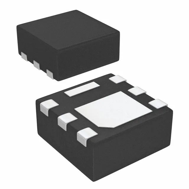
60 V, 18.5 A N-channel — the power envelope for this DFN2020 FET
The 17 mOhm maximum on-resistance at 11 A with 10 V gate drive sets the conduction loss floor for the BOM thermal budget — at 11 A the I²R loss is about 2 W, which the 11.5 W package dissipation rating can handle with adequate copper on the drain pad.
The 8 nC total gate charge at 4.5 V means a 3.3 V MCU GPIO can switch this FET at moderate frequencies without an external gate driver — the GPIO's 10-20 mA source capability charges the gate in under 1 µs.
175°C junction rating — headroom for high-ambient power designs
The -55°C to 175°C operating junction temperature range exceeds the typical 150°C limit of many small-package FETs. In a sealed 85°C ambient with 2 W dissipation, the junction stays below 125°C — well within the 175°C ceiling. This margin matters for under-hood automotive, industrial motor drives, and hot-swap power supplies where the ambient temperature can spike.
DFN2020 package — board area savings with thermal design constraints
The 6-PQFN (2x2) DFN2020 package measures 2 mm × 2 mm, roughly half the footprint of an SO-8. Without that copper plane, the 11.5 W dissipation rating drops significantly; the effective RthJA depends on PCB copper area.
ROHS3 compliant per the listing.