Gate drive and switching considerations
The gate charge is 140 nC at 5 V, which sets the driver energy per switching cycle. The input capacitance is 3700 pF at 25 V drain-source, which together with the gate resistance determines the switching speed and turn-on/turn-off delay. The maximum gate-source voltage is ±16 V, so a 10 V or 12 V gate drive rail is safe, but a 15 V rail would exceed the rating.
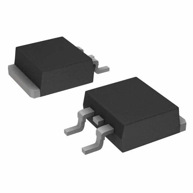
Housed in a D2PAK (TO-263-3) surface-mount package with a large exposed drain tab. The tab is the thermal path to the board — a copper pour on the top and bottom layers with vias is needed to keep junction temperature below 175°C at full load. The package reworks cleanly with hot air if the board has adequate copper soak. Power dissipation is rated at 3.8 W in still air at 25°C ambient, and 200 W when the case is held at 25°C — the real limit in a design is the board's ability to sink heat.