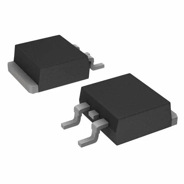
The D2PAK (TO-263) package puts the drain on the exposed tab, so the thermal path runs through the board copper, not the air. This is a part you solder down with a wide drain pad and plenty of vias, not something you socket in the field.
Gate charge and drive voltage — sizing the gate driver
Gate charge is 140 nC at 5 V, and the drive voltage range for minimum Rds(on) is 4.3 V to 10 V.
Temperature range and derating — where this FET lives
The 175°C max is the ceiling for the silicon, not the solder joint — the D2PAK lead finish is matte tin, so the board-level reliability at sustained high temperature depends on the PCB laminate and solder alloy. The 160 A rating is at Tc=25°C; at 100°C case temperature you derate to about 110 A, still a lot of current for a surface-mount package if the board copper does the heat spreading.