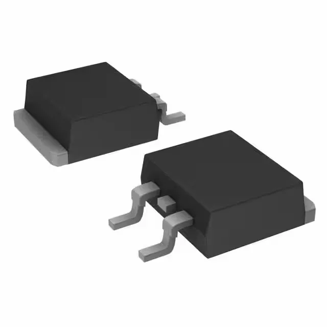
It is built with standard MOSFET (Metal Oxide) technology and packaged in a surface-mount D2PAK (TO-263-3) with an exposed tab for thermal management.
13.9 mOhm on-resistance — what it drives for the BOM
The maximum on-resistance of 13.9 mOhm, specified at a drain current of 31 A and a gate drive of 10 V, determines the conduction losses that set the thermal budget. At 31 A, the I²R loss reaches roughly 13.4 W, which must be dissipated through the D2PAK tab and PCB copper.
NRND — no longer recommended for new designs
This means Infineon has flagged it for eventual discontinuation, though it remains available in the supply channel for existing production runs and service repairs. For new designs, evaluate a current-production N-channel MOSFET in the same voltage class and package.
The input capacitance of 1420 pF at a drain-source voltage of 25 V is typical for a 55 V class device in this current range and influences the gate drive design.