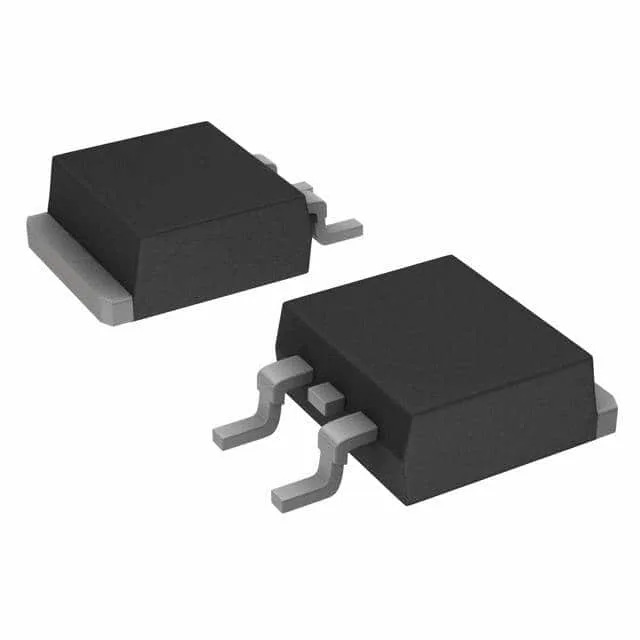
324 nC gate charge — the driver budget for switching frequency
To switch this FET in 100 ns, the gate driver must source over 3 A peak. The input capacitance of 10820 pF at 25 V drain-source reinforces the same message: this is a large-die part designed for low-frequency hard switching (up to maybe 50–100 kHz) or for synchronous rectification where the FET is on most of the cycle. A small SOT-23 gate driver will struggle; plan for a dedicated driver with at least 4 A peak source-sink capability.
175 °C junction — military-temperature silicon in a D2PAK
The 175 °C Tj max is unusual for a 40 V trench MOSFET — most competitors stop at 150 °C. This part can live in an engine bay, a hot-swap supply, or a telecom rectifier where the ambient near the FET hits 125 °C.
No last-time-buy window to track, no successor to qualify. The part is ROHS3 compliant.