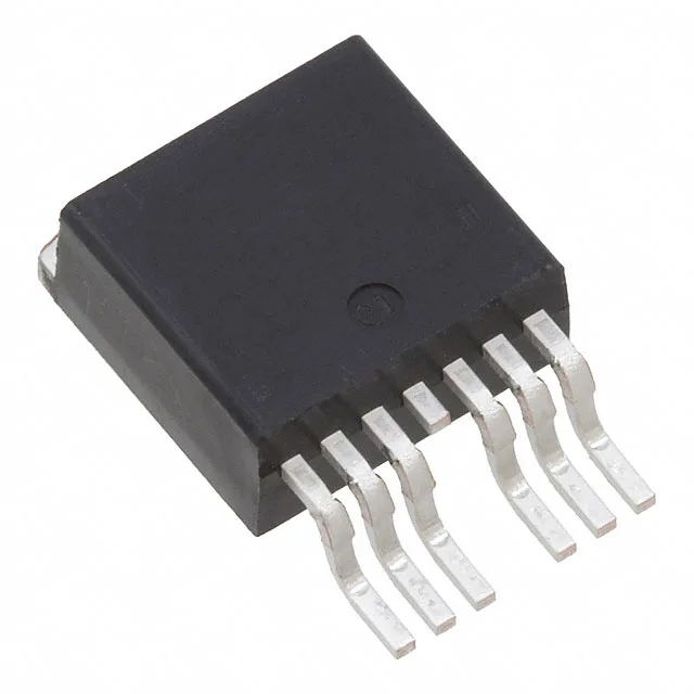
1 mOhm Rds(on) at 100 A — the switching loss floor
The IRFS7434TRL7PP: The device is rated for a drain-to-source voltage of 40 V and a continuous drain current of 240 A at a case temperature of 25 °C.
Gate charge and input capacitance — what the driver sees
The total gate charge is 315 nC at 10 V, and the input capacitance is 10250 pF at a 25 V drain-source bias. These numbers tell the gate-driver designer what current is needed to hit the target switching frequency. A 315 nC gate charge at 100 kHz switching requires an average gate drive current of about 31.5 mA, which is well within the capability of a standard MOSFET driver, but the peak current during the Miller plateau needs to be higher to avoid excessive switching losses.