The 87 nC total gate charge at 10 V means a moderate driver current budget — at 100 kHz switching, the average gate drive current is about 8.7 mA, well within a standard gate driver IC's capability. Input capacitance of 3180 pF at 50 V Vds is typical for this die size; the switching node rise time is set by the driver's source/sink current into this capacitance plus the Miller plateau charge.
175 °C junction — industrial and under-hood margin
The 4 V maximum gate threshold at 100 µA drain current means the device is fully enhanced with a standard 10 V gate drive; it will not turn on with a 3.3 V logic signal.
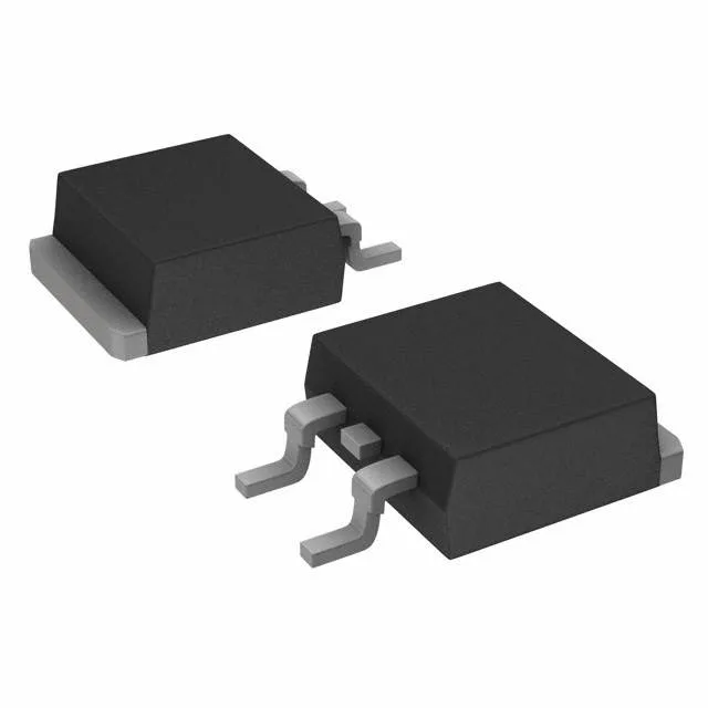
D2PAK footprint and thermal management
A minimum of 6 cm² of 2 oz copper on the top layer is typical for dissipating 140 W at 175 °C junction.