Gate charge and driver budget
The IRFS4321TRLPBF: Total gate charge is 110 nC at 10 V. Input capacitance is 4460 pF at 25 V Vds. This capacitance, combined with the gate charge, sets the switching energy; the designer should verify the driver's sink/source capability against the Qg total and the target rise/fall time.
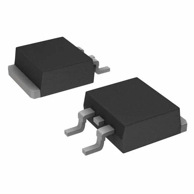
Housed in a D2PAK (TO-263-3) surface-mount package with the tab as the drain connection.
ROHS3 compliant. The ±30 V maximum gate-source rating gives margin for gate-drive transients in noisy environments.