Gate drive and switching — 250 nC Qg at 10 V
The ±20 V maximum gate rating gives headroom for gate-drive overshoot in noisy environments.
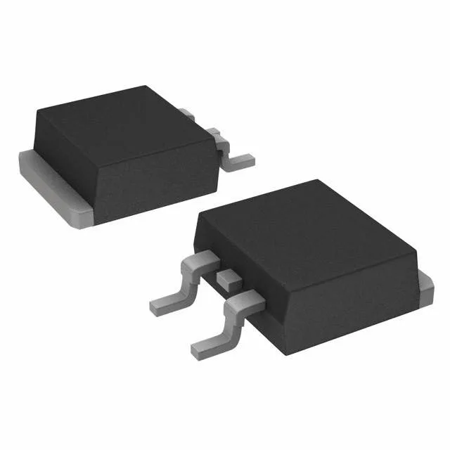
The D2PAK has a large exposed tab — rework requires a preheat zone around 150°C to avoid thermal shock to the die, and the tab solder joint must be inspected for voids; a hot-air station with a wide nozzle works, but the thermal mass means a longer soak than a small-signal SO-8.
ROHS3 compliant. No official second-source or successor is listed, but the D2PAK footprint is standard across the industry — many 100 V N-channel MOSFETs in TO-263 share the same pad layout, though gate charge and Rds(on) vary.