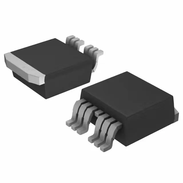
75 V, 240 A — the switching MOSFET for high-current rails
The IRFS3107TRL7PP: The 2.6 mOhm maximum Rds(on) at Vgs=10 V and 160 A sets the conduction loss floor for high-current switching stages.
At 160 A drain current and Vgs=10 V the maximum on-resistance is 2.6 mOhm. That 2.6 mOhm at 160 A means 67 W conduction loss at 25 °C junction — the 370 W package dissipation limit gives headroom for switching loss, but only if the heatsink keeps Tc below 100 °C. The die is sized for this current density; the limiting factor is the D2PAK leadframe's ability to sink heat into the board copper.
240 nC gate charge — driver current budget
Total gate charge at Vgs=10 V is 240 nC. The 9200 pF input capacitance at Vds=50 V means the driver must source a 9.2 nF load per switching edge — a standard totem-pole driver with 2 A peak output handles the transition in roughly 100 ns, but the 240 nC total charge sets the gate-loop energy per cycle.
D2PAK-7 footprint — not the standard TO-263-3
The package is a 7-lead D2PAK (TO-263-7) with six leads plus the tab. The extra leads are typically multiple drain connections or Kelvin source — they reduce package resistance and improve current sharing. The PCB land pattern must match the 7-lead footprint; a standard 3-lead D2PAK pad layout will leave the outer pads unconnected. Surface-mount assembly with the large tab requires a solder-paste stencil that covers the exposed pad for thermal transfer.