13 mOhm Rds(on) in a 2x2 mm footprint — sizing the switch
The IRFHS8242TRPBF is an N-channel HEXFET MOSFET rated for 25 V drain-source and 9.9 A continuous drain at 25 °C ambient, or 21 A referenced to the case.
Gate charge and switching — what the 10.4 nC means for the driver
Input capacitance is 653 pF at 10 V drain-source.
DFN2020 layout — thermal vias and solder paste area
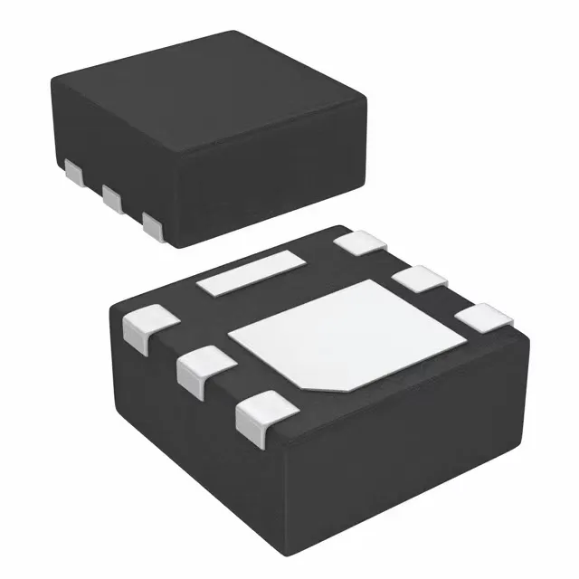
The 6-PQFN (2x2 mm) package, supplier code DFN2020, has an exposed drain pad on the bottom. The 2.1 W Ta dissipation assumes the standard JEDEC 1-inch-square copper pad on a 1 oz board — real-world performance depends on the number and diameter of thermal vias under the pad. For a 2-layer board, at least four 0.3 mm vias filled with solder are typical to pull heat into the inner ground plane. The 0.50 mm pitch on the side leads demands a solder paste stencil aperture that does not bridge to the centre pad.