Total gate charge is 48 nC at 10 V — a moderate figure that lets a standard gate driver (e.g., 1 A peak) switch the FET in under 100 ns.
Thermal and package reality
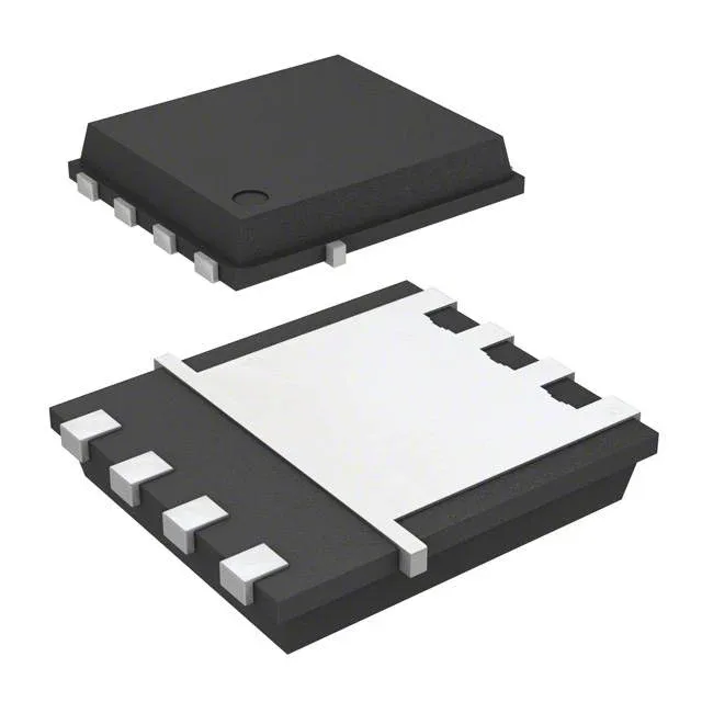
The 8-PowerTDFN (PQFN 3x3) package dissipates 2.8 W at 25 °C ambient when the exposed paddle is soldered to a copper land on the PCB — without that thermal connection the RthJA rises sharply, and the 11 A rating becomes thermally limited long before the silicon hits its 150 °C junction limit. The ±25 V maximum gate rating gives headroom for 12 V or 15 V gate drives without a zener clamp.