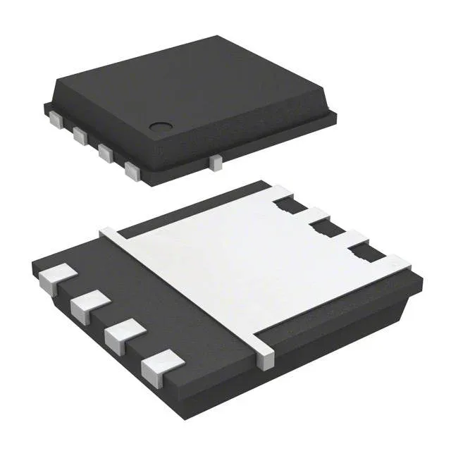
40 V, 85 A N-channel — conduction loss floor at 2.4 mOhm
Gate charge totals 138 nC at 10 V, which determines the driver current needed for the target switching frequency.
Thermal and package — 104 W through the exposed pad
The 0.50 mm pitch of the PQFN-8 demands a solder-paste stencil aperture sized for the pad geometry — a standard reflow profile for lead-free solder applies.
Gate drive and switching — not a logic-level part
The gate threshold voltage is 3.9 V maximum at 100 µA drain current, and the drive voltage range for achieving minimum on-resistance is 6 V to 10 V.