Low Rds(on) for high-current switching
That Rds(on) figure — specified at a high current — tells you the conduction loss stays low even under heavy load, which matters for synchronous rectification stages and low-voltage OR-ing diodes where every milliohm adds to the thermal budget.
Gate charge and drive voltage
Total gate charge is 230 nC at 4.5 V, with a maximum gate-source voltage of ±12 V. The drive voltage range for achieving the minimum Rds(on) is 2.5 V to 10 V — a 5 V logic-level gate drive will turn it on hard enough for most 20 V rails, but the 230 nC Qg means the upstream driver needs to source a few amperes peak to keep switching losses in check at frequencies above 100 kHz.
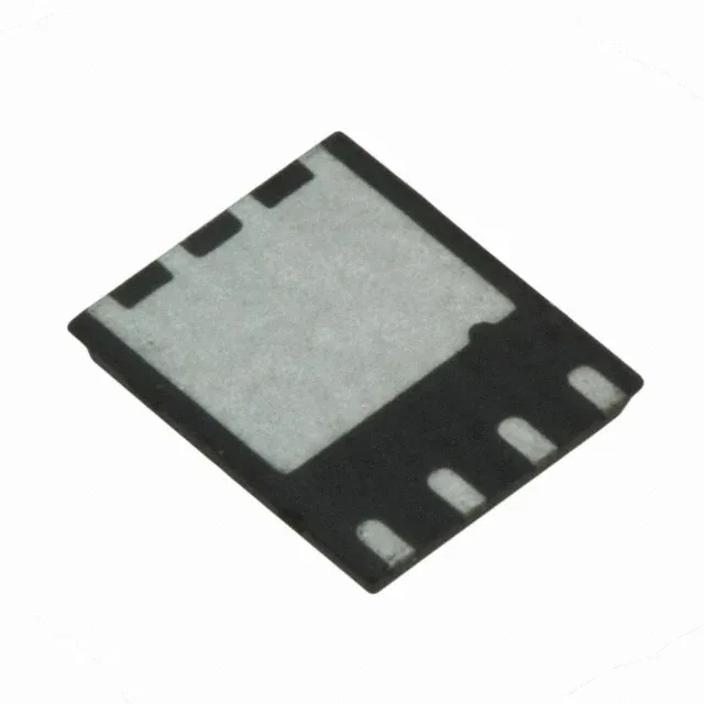
Housed in an 8-PowerVDFN (supplier package 8-PQFN, 5x6 mm), this is a surface-mount part with an exposed paddle on the bottom. The power dissipation rating tells the story: 3.6 W at ambient (Ta) versus 156 W at the case (Tc) — the difference is the thermal resistance of the board. For the 100 A rating to be usable, the PCB must have a large copper area and preferably thermal vias under the paddle to pull heat into an internal plane.
The 150°C Tj max gives headroom for fault conditions like load dumps or stalled fans, but the 3.6 W ambient dissipation limit means the board-level thermal design must be verified at the expected operating temperature.