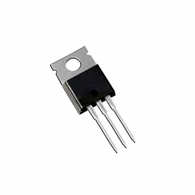
60 V, 195 A N-channel — the conduction-loss benchmark
Gate charge and drive voltage — what the 279 nC Qg means for the driver
Total gate charge is 279 nC at 10 V. That is a heavy gate load — a driver sourcing 2 A peak current will still take roughly 140 ns to charge the gate through the Miller plateau. For switching frequencies above 50 kHz, the gate-driver power dissipation and switching loss in the MOSFET itself become the design constraint, not the Rds(on).
Package and thermal budget — TO-220AB in a 294 W dissipation envelope
Housed in a TO-220-3 (TO-220AB) through-hole package, the IRFB7534PBF is rated for 294 W maximum power dissipation at case temperature 25°C. The 175°C TJ(max) gives headroom above the usual 150°C industrial limit, but the 294 W dissipation rating is only achievable with an adequate heatsink: the tab must be bolted to a thermal mass sized for the average power loss, not the peak. Input capacitance Ciss is 10034 pF at 25 V drain-source — typical for a die this large, and a factor in switching loss at higher frequencies.
ROHS3 compliant. No stock-holding claim; quoted per BOM quantity.