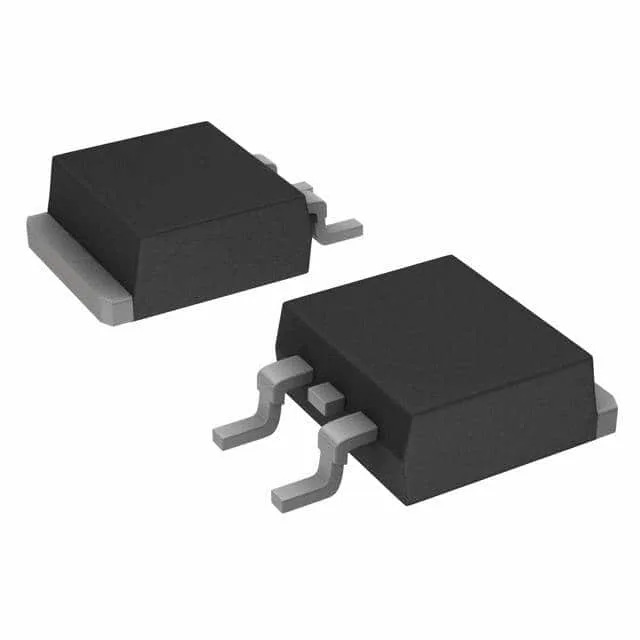
P-Channel 100 V switch for high-side loads
The IRF9530NSTRLPBF is a P-Channel enhancement-mode HEXFET MOSFET in the D2PAK (TO-263) surface-mount package, rated for 100 V drain-source and 14 A continuous drain current. It is designed for high-side switching applications where a P-Channel device eliminates the need for a charge-pump gate driver — the gate is simply pulled low to turn the FET on.
Maximum on-resistance is 200 mOhm at a gate-source voltage of 10 V and 8.4 A drain current. This is the figure to use for worst-case conduction loss calculations at the rated gate drive — at lower Vgs the Rds(on) rises, so the 10 V drive rail is effectively mandatory to achieve the rated current.
Thermal limits and package power dissipation
Power dissipation is rated at 3.8 W at 25 °C ambient (Ta) and 79 W at the case (Tc). The large D2PAK tab carries the heat — the board copper area under the tab sets the real thermal resistance. For continuous 14 A operation, a heatsink or a substantial PCB copper pour is expected.
This is a moderate gate charge for a 14 A FET — a standard gate driver with a few hundred mA peak current will switch it in the tens of nanoseconds. The 58 nC figure is the basis for the driver's average current budget at the target switching frequency.