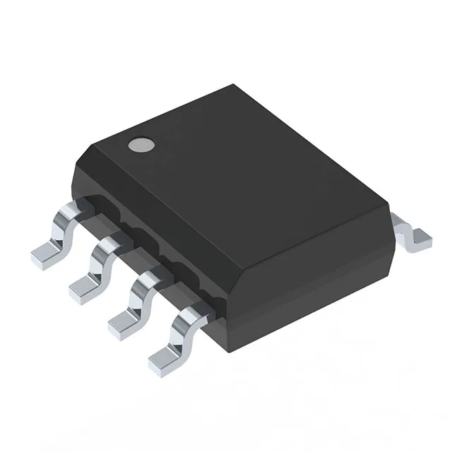
P-channel load switch in an SO-8
The 8.5 mOhm maximum on-resistance at 20 V gate drive keeps conduction loss low in high-side switching, battery-ORing, and load-switch applications where a P-channel simplifies the gate drive because the source is tied to the supply rail.
At 12 A the 8.5 mOhm channel resistance produces about 1.2 W of conduction loss (I²R), which sits within the 2.5 W package power dissipation limit at 25°C ambient.