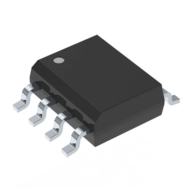
P-channel 30V MOSFET in SOIC-8 — load-switch fit
Gate charge is 14nC at 10V, which keeps the switching driver load modest at moderate frequencies.
Rds(on) is specified at 59mOhm max with Vgs=10V and Id=5.4A. That 59mOhm figure is the conduction-loss anchor for a 5A load — expect about 1.5W dissipation at full current before derating. The gate charge of 14nC at 10V means a gate driver sourcing 1A can switch the FET in roughly 14ns, though the practical edge rate is limited by the gate-driver loop inductance and the 386pF input capacitance at 25V Vds.
Thermal envelope and package reality
The 2.5W power dissipation at 25°C ambient is the package-limited ceiling in free air — a 5.4A load at full Rds(on) pushes 1.5W, leaving 1W of thermal headroom before hitting the 150°C junction limit. The SOIC-8 body (0.154-inch width) is a standard footprint; the 8-SO supplier device package matches the common SO-8 land pattern.