The headline on-resistance of 4.8 mOhm (max at 18 A, 10 V Vgs) sets the conduction-loss floor for a low-voltage synchronous buck or load switch — but that figure assumes a 10 V gate drive, not the 4.5 V threshold. At 4.5 V drive the Rds(on) rises; the datasheet curve tells you how much. The 26 nC total gate charge at 4.5 V means a 1 A gate-driver can switch this FET at roughly 38 kHz before the driver's average current budget is consumed.
30 V / 18 A — what the ratings actually mean for your rail
The 18 A continuous drain rating is specified at 25 °C case temperature (Ta), not ambient — on a typical 1 oz copper, 1-square-inch pad on a 2-layer board, the actual current you can sustain is lower. The 2.5 W max power dissipation at 25 °C ambient is the thermal budget you have to work with; the SO-8 package's junction-to-ambient thermal resistance means the PCB copper area does the real heat sinking. For a 12 V input rail or a 5 V point-of-load converter, the 30 V drain rating gives about 1.5× derating margin — adequate for most non-automotive rails.
Package and footprint — standard SO-8, thermal via pattern matters
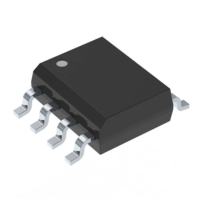
The 8-SOIC package (0.154-inch body width, 3.90 mm) uses the standard SO-8 footprint. The supplier device package is 8-SO. The gate charge of 26 nC at 4.5 V is moderate — a typical 1 A gate driver can handle switching frequencies up to about 38 kHz before the average gate-drive current becomes a concern.