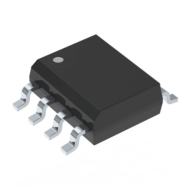
100 V N-channel in an SOIC-8 — conduction loss and gate drive
Gate charge and switching — 39 nC at 10 V
This is a moderate charge for a 100 V part — a standard gate driver with 1 A peak output can switch it at 50–100 kHz without excessive driver dissipation.
Temperature range — military-grade junction rating
The 2.5 W power dissipation at 25°C ambient is the board-level limit in still air — in a 150°C junction environment the allowable dissipation drops to near zero, so the thermal design must rely on the PCB copper to sink heat.
It is ROHS3 compliant.