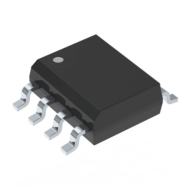
Complementary N/P-channel in one SO-8
The IRF7343TRPBF integrates an N-channel and a P-channel MOSFET in a single 8-SOIC package, rated for a drain-to-source voltage of 55 V. The N-channel side handles 4.7 A continuous drain current; the P-channel side is rated at 3.4 A. On-resistance is 50 mOhm maximum for the N-channel at Vgs = 10 V and 4.7 A. This dual configuration lets one device replace two separate MOSFETs in half-bridge topologies, synchronous rectifier stages, or bidirectional load switches — cutting component count and PCB area.
Thermal budget in SO-8
Maximum power dissipation is 2 W in the SO-8 package. That 2 W ceiling sets the practical continuous current well below the 4.7 A / 3.4 A ratings unless the board provides generous copper area on the drain pads. For a 55 V rail, the Rds(on) at elevated junction temperature rises roughly 50 % above the 25 °C value — factor that into the thermal loop when sizing the load.
The gate charge is moderate — a standard 1 A gate driver can switch the pair at 100–200 kHz without excessive drive loss.