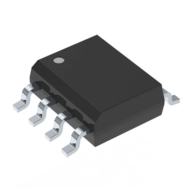
Dual P-channel 30 V switch in an SO-8
It comes in an 8-SOIC package (0.154-inch body width) and is built on Infineon's HEXFET trench process. This simplifies the BOM for battery-powered load switches or low-voltage rail switching.
On-resistance and switching parasitics
At the logic-level threshold the Rds(on) will be higher — budget the conduction loss against the actual gate voltage your design provides. Maximum power dissipation is 2 W in the SO-8 package. The junction-to-ambient thermal resistance is set by the copper area on the drain pads — a 1-inch² pad on a 2-oz copper board is the typical reference for the 2 W rating.
This covers military, avionics, and downhole applications where the ambient can exceed 85 °C, as well as outdoor telecom and engine-bay environments. The wide span also provides derating headroom for conduction and switching losses.
It is ROHS3 compliant.