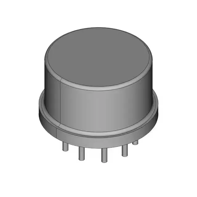
Infineon Technologies IRF6713STRPBF — Discrete Semiconductors

IRF6713STRPBF N-Channel MOSFET, 25V, 3mOhm, DirectFET

MPNIRF6713STRPBF
Active

Infineon IRF6713STRPBF N-Channel MOSFET, DirectFET series, 25 V drain-source, 22 A / 95 A switching current, 3 mOhm Rds(on) at 10 V, ±20 V gate drive, surface mount.

$1.00Ref. price · indicative, final on quote
StockContact for availability
MOQ1 pcs
  • 100% new & originalTraceable channels only — no refurbs, no pulls, no remarked parts.
  • Date & lot codes on quoteStated per line before you commit; label photos on request.
  • MSL-compliant ESD packingMoisture-sealed bags with indicator cards; reels photo-verified.
  • PayPal buyer protectionPay by T/T, PayPal or Payoneer — card payments covered end to end.

Specifications

IRF6713STRPBF Technical Specifications
ParameterValue
SeriesDirectFET™
FET typeN-Channel
Mounting_typeSurface Mount
Operating temperature high-40°C to 150°C(TJ)
Vgs±20 V
Power_w2.2
Package_typeBulk
Capacitance_uf0.0029
Product_statusActive
Supply_voltage_v25.0
Vgs(Th) (Max) @ id2.4 V @ 50µA
Switching_current_a22.0
Rds on (Max) @ id, vgs3mOhm @ 22 A, 10 V
Gate charge (Qg) (Max) @ vgs32 nC @ 4.5 V

Product details

DirectFET N-channel for low-voltage high-current switching

The IRF6713STRPBF is an N-channel MOSFET from Infineon's DirectFET series, rated for 25 V drain-source and a continuous drain current of 22 A (95 A pulsed) in a surface-mount can-style package.

That means the BOM line is safe for new designs and production ramp without sourcing risk from a looming EOL.

Low gate-charge profile for fast switching

Total gate charge is 32 nC at 4.5 V gate drive. At a 500 kHz switching frequency the gate driver delivers about 16 mA average — well within the capability of a standard half-bridge driver IC. The ±20 V maximum gate-source rating gives headroom for driving the FET from a 12 V regulated rail without worrying about oxide breakdown during transients.

Thermal and package reality for the layout

The DirectFET package is a copper can with the drain on the top-side tab — the PCB copper area under the can sets the junction-to-ambient thermal resistance. The datasheet lists 2.2 W power dissipation, but that figure assumes a standard footprint. For a 25 V, 22 A load switch or synchronous rectifier stage, the layout engineer should allocate a flooded copper region on the top layer under the can and vias to an inner-plane copper pour to keep Tj below the 150 °C maximum junction temperature.

Frequently asked questions

What is the Rds(on) of IRF6713STRPBF at 4.5 V gate drive?

The maximum Rds(on) is 3 mOhm at 4.5 V gate drive with 22 A drain current. This is the same value specified at 10 V, meaning the FET saturates fully at logic-level gate voltages.