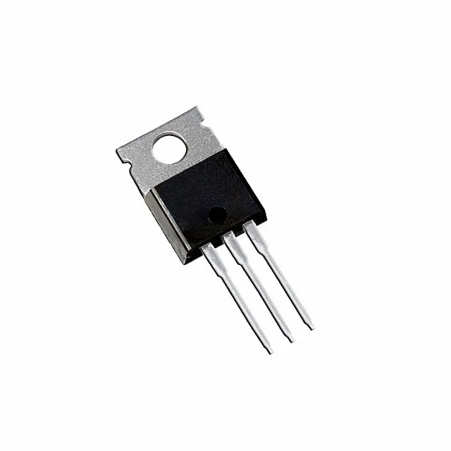
Infineon Technologies IRF630NPBF

IRF630NPBF N-Channel MOSFET, 200V 9.3A TO-220AB HEXFET

MPNIRF630NPBF
End of Life

IRF630NPBF, HEXFET® N-Channel MOSFET, 200 V drain-source, 9.3 A continuous drain current, 300 mOhm Rds(on) at 10 V gate drive, 35 nC gate charge, TO-220AB through-hole, -55°C to 175°C junction temperature.

$1.06Ref. price · indicative, final on quote
PackagingTO-220-3
StockContact for availability
MOQ1 pcs
  • 100% new & originalTraceable channels only — no refurbs, no pulls, no remarked parts.
  • Date & lot codes on quoteStated per line before you commit; label photos on request.
  • MSL-compliant ESD packingMoisture-sealed bags with indicator cards; reels photo-verified.
  • PayPal buyer protectionPay by T/T, PayPal or Payoneer — card payments covered end to end.

Specifications

IRF630NPBF Technical Specifications
ParameterValue
SeriesHEXFET®
FET typeN-Channel
Mounting typeThrough Hole
Drain to source voltage200 V
Drive voltage (Max rds on, min rds on)10V
Current - continuous drain (Id) @ 25°C9.3A (Tc)
Power dissipation82W (Tc)
Operating temperature-55°C ~ 175°C (TJ)
PackageTube
Vgs±20V
TechnologyMOSFET (Metal Oxide)
CaseTO-220-3
Vgs(th) (Max) @ id4V @ 250µA
Rds on (Max) @ id, vgs300mOhm @ 5.4A, 10V
Gate charge (Qg) (Max) @ vgs35 nC @ 10 V
Input capacitance (Ciss) (Max) @ vds575 pF @ 25 V

Product details

Package and mounting

The IRF630NPBF is an N-channel enhancement-mode MOSFET from the HEXFET series, built on a planar stripe DMOS process that gives it a 200 V drain-source breakdown and a continuous drain current rating of 9.3 A at 25°C case temperature. The 300 mOhm maximum on-resistance at Vgs=10 V and 5.4 A sets the conduction loss floor — at 5 A the dissipation runs about 7.5 W, which the TO-220AB package can handle with a modest heatsink before the junction hits 175°C. Gate charge totals 35 nC at 10 V, so a gate driver sourcing 1 A can switch the FET in about 35 ns — fast enough for a 100 kHz SMPS primary, but the 575 pF input capacitance at 25 V means the driver sees a capacitive load that needs a low-impedance loop back to the source pin.

Thermal and switching — the numbers that decide the heatsink and the driver

The 82 W maximum power dissipation at Tc=25°C is a case-temperature-limited figure — real-world dissipation at a 100°C case drops to about 35 W, which is where the TO-220 tab bolted to a finned heatsink earns its keep. Threshold voltage is 4 V maximum at 250 µA drain current, so a 5 V logic gate drive will barely turn it on — the datasheet specifies 10 V drive for the rated Rds(on), and anything below 8 V risks operating in the linear region with high dissipation. The ±20 V maximum gate-source rating gives headroom for gate-drive overshoot, but a 10 V drive is the sweet spot — driving to 15 V gains no Rds(on) improvement and eats into the margin on the gate oxide.

Where the scorch mark tells you it failed — repair bench reality

On a failed offline flyback supply, the IRF630NPBF typically dies shorted drain-to-source when the primary-side snubber or the reflected voltage exceeds 200 V — the scorch mark on the TO-220 tab is usually at the drain pin exit.

Frequently asked questions

What is the Rds(on) of IRF630NPBF at 10 V gate drive?

The maximum Rds(on) is 300 mOhm at Vgs=10 V and Id=5.4 A. This is the on-resistance that sets the conduction loss budget for the design — at 5 A the dissipation is about 7.5 W, so a heatsink is expected for continuous operation.

What is the maximum drain current for IRF630NPBF?

The continuous drain current is 9.3 A at 25°C case temperature. Derate linearly above 25°C — at 100°C case temperature the usable current drops to roughly 6 A, limited by the junction temperature ceiling of 175°C.