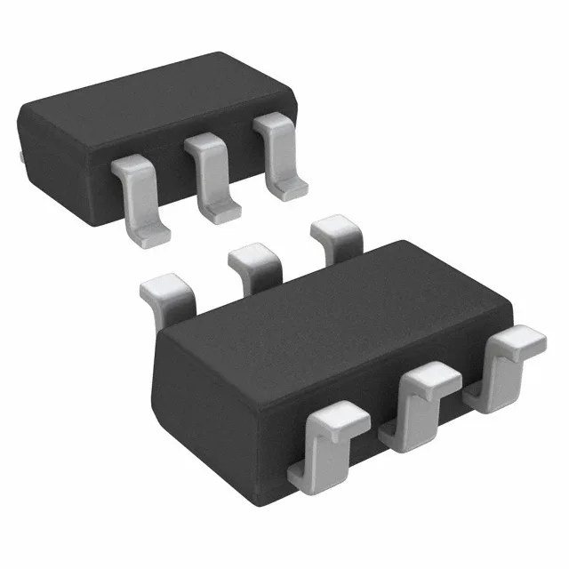
P-channel load switch in a TSOP-6 footprint
Gate threshold voltage maxes at 3 V at 250 µA drain, so a 4.5 V logic signal can start turning the FET on, but the 37 nC total gate charge at 10 V tells you the driver needs to source enough current to hit the target switching speed. Input capacitance is 1110 pF at 25 V Vds — a figure that sets the driver's peak current requirement for the rise and fall edges. The ±20 V Vgs max gives headroom for gate ringing on long PCB traces.
Thermal reality in the Micro6 package
The 2 W power dissipation at 25°C ambient is the absolute limit in still air; derate aggressively above that temperature. The Micro6™ (TSOP-6) footprint has a small copper pad area under the drain tab — the datasheet's thermal resistance figure assumes a 1-inch-square pad on a 2-layer board. If your board is dense or the ambient runs to 85°C, budget for a lower continuous current than the 3.4 A headline number.