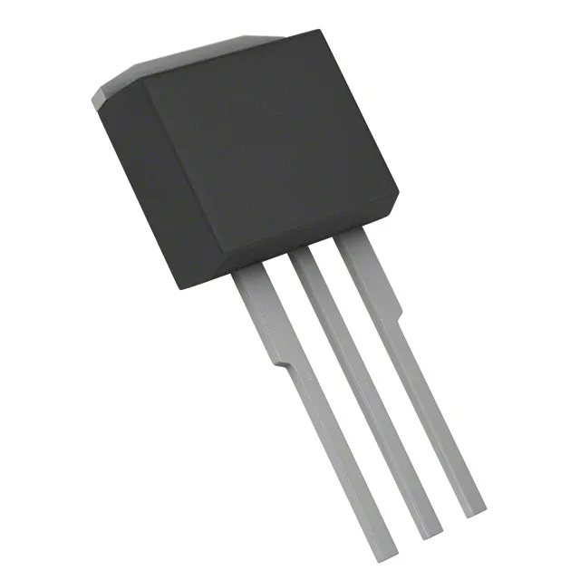
P-channel 55V 42A — conduction loss and package
Gate charge and switching drive
Total gate charge is 180 nC at 10 V, with input capacitance at 3500 pF measured at 25 V drain-source.
Temperature range and power dissipation
Maximum power dissipation is 170 W at case temperature, derated above that point per the datasheet curve. The TO-262 through-hole package (I²Pak) provides a low thermal resistance path to a heatsink via the exposed metal tab.
It is ROHS3 compliant, and the TO-262 package is standard through-hole for automated or manual assembly.