What the gate charge and capacitance mean for the driver
The 220 nC figure also sets the gate-drive power loss: at 100 kHz, the driver dissipates about 220 mW just charging and discharging the gate, which matters for the driver's thermal budget.
Temperature range and the real current limit
The 140 A continuous rating is at 25°C case temperature — in a real board with a heatsink, the allowable current derates as the junction rises. At 100°C case temperature, the current capability drops to roughly 100 A, depending on the thermal resistance of the mounting interface. The 175°C maximum junction lets the part survive overload conditions that would kill a 150°C-rated MOSFET, but continuous operation near that ceiling requires a substantial heatsink and forced airflow.
Active production — no LTB scramble on this BOM line
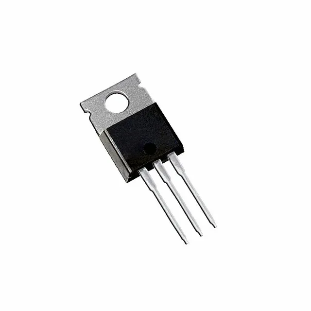
For a repair bench or a production BOM, this means the part can be sourced through standard distribution without worrying about a looming obsolescence window. The TO-220AB package is a common footprint, so second-sourcing from other manufacturers with compatible pinouts is straightforward if dual-source security is needed.