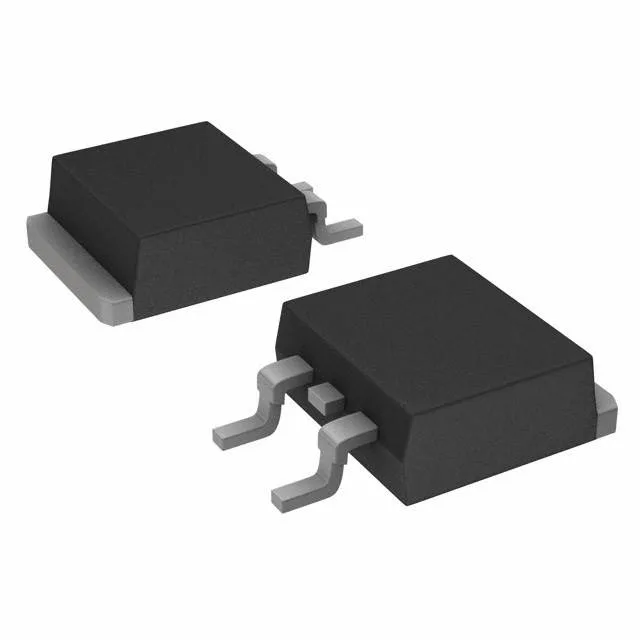
3.3 mOhm at 75 A — the conduction-loss floor
The headline figure is the 3.3 mOhm maximum on-resistance at Vgs=10 V and 75 A — this sets the conduction-loss floor for a high-current switching stage. At 75 A, I²R losses sit at roughly 18.6 W, which the 300 W package dissipation can handle with adequate heatsinking.
290 nC gate charge — driver selection matters
Gate charge totals 290 nC at Vgs=10 V. That is a heavy load for a gate driver — expect to budget a driver capable of sourcing at least 2 A peak to keep switching transitions under 150 ns. The 7960 pF input capacitance at Vds=25 V reinforces the same point: the driver sees a large capacitive load, and rise/fall times will be dominated by the driver's current capability.
D2PAK footprint and thermal path
The 300 W dissipation rating assumes the tab is soldered to a copper plane of adequate area — a 1 oz copper pad of at least 25 mm x 25 mm on a 2-layer board gets you into the 40-50 °C/W RthJA range.