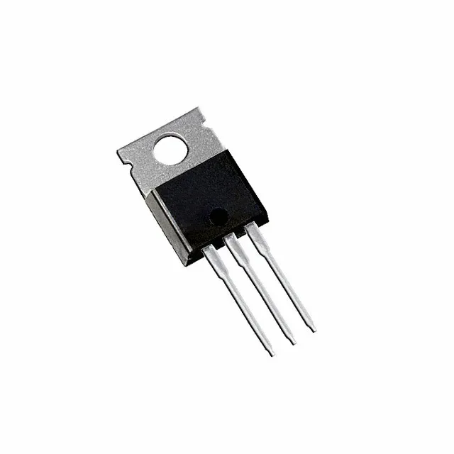
Through-hole power MOSFET for high-current switching
Operating junction temperature spans -55 to 175 °C, suiting it for industrial and automotive environments where the thermal cycling is aggressive.
Total gate charge is 270 nC at 10 V — a standard 1 A gate driver will take roughly 270 ns to switch the FET, so plan for a driver with at least 2 A peak source/sink capability if the target switching frequency exceeds 20 kHz.
The TO-220AB package has a metal tab that is electrically common with the drain — the PCB or heatsink pad must be isolated or the system must tolerate the drain potential on the heatsink. Maximum power dissipation is 300 W at case temperature, but the real thermal limit depends on the heatsink's thermal resistance; a 1 °C/W heatsink keeps the junction below 175 °C at 100 W dissipation.