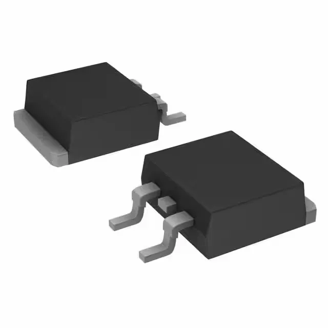
A 40 V, 180 A HEXFET in a D2PAK — what it was designed for
Any stock available in the open market is new-old-stock or surplus inventory pulled from distributor channels or OEM overstocks. For a production BOM that still calls out this exact order code, sourcing now depends entirely on independent distribution and verified surplus lots. Date-code provenance matters here — stock surfacing years after the official end-of-life should be inspected for authenticity and shelf-life condition, particularly given the MSL sensitivity of the D2PAK package.
The 3.7 mOhm Rds(on) at 10 V gate drive is the headline efficiency figure — in a 100 A load, that resistance yields roughly 37 W conduction loss at the die, which the 220 W package rating can handle with adequate heatsinking and airflow. The 40 V Vdss leaves limited headroom for a 24 V nominal rail with inductive ringing — a 30% derating guideline would put the practical bus voltage around 28 V maximum, so a 24 V system with clean layout is fine, but a 36 V nominal bus would exceed the derating margin.
The part is a single-die N-channel MOSFET with a ±20 V maximum gate-source voltage, so the gate drive must be clamped or limited to stay within that window.