Gate charge and driver budget
Total gate charge is 270 nC at 10 V — a standard MCU GPIO or a 0.5 A gate driver will struggle to switch this FET at any useful frequency. Plan for a dedicated gate driver capable of 2 A peak source/sink to keep the switching edges clean and the cross-conduction interval short. The input capacitance of 9700 pF at 50 V Vds confirms the driver needs to deliver a stiff gate voltage slew rate.
Package reality — rework and thermal management
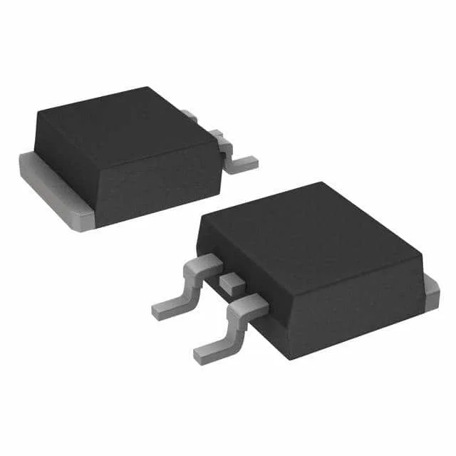
The large copper pad on the bottom soaks heat fast — a standard hot-air station without bottom preheat will struggle to lift this part without cooking the board. Use a preheat plate at 150 °C and a wide-tip soldering iron for the tab solder joint. Orientation is marked by a bevel on the top edge — find pin 1 before the hot air goes on.