0.58 mOhm at 10 V — the conduction-loss floor for high-current rails
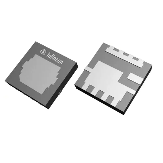
The Infineon IQE006NE2LM5CGSCATMA1 is an N-channel OptiMOS™ 5 power MOSFET rated for 25 V drain-source and a max on-resistance of 0.58 mOhm at 20 A with 10 V gate drive. That sub-milliohm figure is the headline: it means the conduction loss at 50 A is under 1.5 W, which keeps the die temperature manageable even without heroic heatsinking. The 310 A continuous drain rating at the case (Tc) tells you the silicon can handle the current — the real limit will be the PCB's ability to pull heat out of the PG-WHTFN-9-1 package's exposed pad.
4.5 V or 10 V gate drive — matching the driver to the rail
The datasheet specifies Rds(on) at both 4.5 V and 10 V drive voltages. If your design runs a 5 V logic rail and the gate driver is a simple GPIO, the 4.5 V spec is the one that matters — the FET will still turn on hard, but the on-resistance will be higher than the 10 V figure. For the full 0.58 mOhm, you need a 10 V gate supply. The gate charge of 82 nC at 10 V means a driver capable of sourcing a few amps peak will switch this FET at tens of kilohertz without excessive cross-conduction.
The 150°C ceiling gives enough headroom for the 2.1 W dissipation at the board (Ta) or 89 W at the case (Tc) before the silicon hits its limit. The 2 V max gate threshold at 250 µA means the FET is fully off below about 1.5 V, so a 3.3 V logic rail will not accidentally turn it on during power-up sequencing.
Package and footprint — PG-WHTFN-9-1 thermal reality
The 0.58 mOhm Rds(on) is only achievable if the board can sink the heat — a two-layer board with minimal copper will let the junction temperature climb well above the 150°C limit at high current. The input capacitance of 5453 pF at 12 V is moderate; the gate driver sees a capacitive load that is easy to drive at moderate frequencies, but at 100 kHz+ the switching losses from charging and discharging that capacitance start to add up.