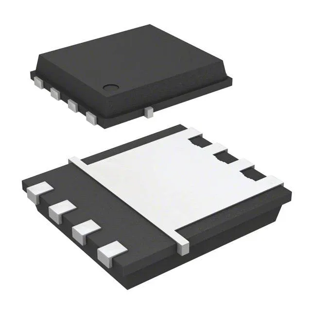
Infineon Technologies IPZ40N04S53R9ATMA1

IPZ40N04S53R9ATMA1 OptiMOS-5 N-Channel MOSFET, 40 V, 89 A

MPNIPZ40N04S53R9ATMA1
End of Life

Infineon OptiMOS™-5 IPZ40N04S53R9ATMA1 N-Channel MOSFET, 40 V Vdss, 89 A Id, 3.9 mOhm Rds(on) @ 20 A / 10 V, 25 nC Qg, PG-TSDSON-8-33, -55 to 175°C, AEC-Q101.

$0.97Ref. price · indicative, final on quote
Packaging8-PowerTDFN
StockContact for availability
MOQ1 pcs
  • 100% new & originalTraceable channels only — no refurbs, no pulls, no remarked parts.
  • Date & lot codes on quoteStated per line before you commit; label photos on request.
  • MSL-compliant ESD packingMoisture-sealed bags with indicator cards; reels photo-verified.
  • PayPal buyer protectionPay by T/T, PayPal or Payoneer — card payments covered end to end.

Specifications

IPZ40N04S53R9ATMA1 Technical Specifications
ParameterValue
SeriesOptiMOS™-5
FET typeN-Channel
Mounting typeSurface Mount
Drain to source voltage40 V
Drive voltage (Max rds on, min rds on)7V, 10V
Current - continuous drain (Id) @ 25°C89A (Tj)
Power dissipation58W (Tc)
Operating temperature-55°C ~ 175°C (TJ)
GradeAutomotive
PackageTape & Reel (TR); Cut Tape (CT)
Vgs±20V
TechnologyMOSFET (Metal Oxide)
QualificationAEC-Q101
Case8-PowerTDFN
Vgs(th) (Max) @ id3.4V @ 21µA
Rds on (Max) @ id, vgs3.9mOhm @ 20A, 10V
Gate charge (Qg) (Max) @ vgs25 nC @ 10 V
Input capacitance (Ciss) (Max) @ vds1737 pF @ 25 V

Product details

3.9 mOhm on-resistance — what it buys the 12 V bus

The IPZ40N04S53R9ATMA1 is an Infineon OptiMOS™-5 N-channel MOSFET rated for 40 V drain-source and 89 A continuous drain at 25°C junction. The headline figure is a maximum 3.9 mOhm Rds(on) at 20 A with 10 V gate drive — that keeps conduction loss under 0.8 W at 20 A, which is the difference between a heatsink and a copper-pour-only layout in an automotive ECU.

Gate charge and switching speed

Total gate charge is 25 nC at 10 V. For a 100 kHz switching regulator, that means the gate driver needs to source about 2.5 mA average current — well within a standard MOSFET driver's capability. The input capacitance (Ciss) is 1737 pF at 25 V drain, which sets the Miller plateau duration and the turn-on/turn-off delay through the driver's source/sink impedance.

Automotive grade and temperature range

The 175°C ceiling is critical for under-hood or high-side switch positions where ambient can exceed 125°C and self-heating from conduction loss pushes the die further.

Package and footprint notes

Supplied in the PG-TSDSON-8-33 package — an 8-lead PowerTDFN with an exposed drain pad on the bottom. The 58 W maximum power dissipation assumes that pad is tied to a suitable heatsink plane; without it, the junction-to-ambient thermal resistance rises sharply and the current rating derates.

Frequently asked questions

What is the Rds(on) of IPZ40N04S53R9ATMA1?

Maximum on-resistance is 3.9 mOhm at 20 A drain current with 10 V gate drive. At 7 V gate drive the Rds(on) is higher — the datasheet specifies drive voltage for max Rds(on) as 10 V, with a minimum recommended drive of 7 V.

Is IPZ40N04S53R9ATMA1 AEC-Q101 qualified?

Yes, it carries AEC-Q101 qualification, which is the automotive stress-test standard for discrete semiconductors. This is the qualification tier required for Tier-1 automotive BOM approval.

What package does IPZ40N04S53R9ATMA1 come in?

It comes in an 8-lead PowerTDFN package, supplier device package code PG-TSDSON-8-33.

What is the gate charge of IPZ40N04S53R9ATMA1?

Total gate charge (Qg) is 25 nC maximum at 10 V gate drive. This is a moderate Qg for a 40 V / 89 A MOSFET — it keeps switching losses manageable at frequencies up to a few hundred kHz.