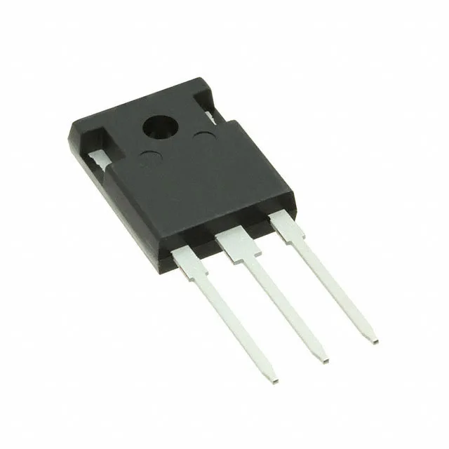
80 mOhm Rds(on) and 167 nC gate charge — the trade-off
The IPW65R080CFDFKSA2: The 80 mOhm figure is the conduction-loss floor at 25 °C junction; at 125 °C junction it roughly doubles, so budget the thermal loop with that headroom. Input capacitance Ciss is 5030 pF at 100 V drain bias — the Miller plateau will be substantial, so the driver's sink current and the gate loop inductance determine the turn-off loss more than the Rds(on) does.
Active production — no scavenger hunt needed
It is ROHS3 compliant, and the TO-247-3 through-hole package suits high-reliability soldering processes and field-serviceable power stages where a rework station is the norm.
The 650 V Vdss gives you 1.6× derating on a 400 V DC bus — enough margin for the ringing on a hard-switched half-bridge without reaching for a 700 V or 800 V part that would have higher Rds(on). The 391 W power dissipation at case temperature is the theoretical limit with an infinite heatsink — in practice the thermal pad area and airflow set the real ceiling.