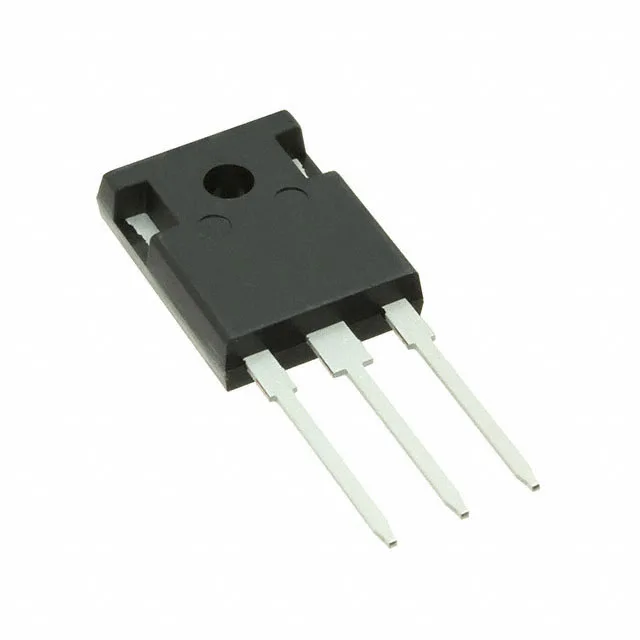
Infineon Technologies IPW65R022CFD7AXKSA1 — Logic ICs

Infineon IPW65R022CFD7AXKSA1 CoolMOS N-Ch 650V 96A MOSFET

MPNIPW65R022CFD7AXKSA1
End of Life

Infineon CoolMOS™ IPW65R022CFD7AXKSA1, N-Channel MOSFET, 650 V Vdss, 96 A Id, 22 mOhm Rds(on) @ 10 V, 234 nC Qg, TO-247-3 through hole, -40°C to 150°C TJ.

$22.27Ref. price · indicative, final on quote
PackagingTO-247-3
StockContact for availability
MOQ1 pcs
  • 100% new & originalTraceable channels only — no refurbs, no pulls, no remarked parts.
  • Date & lot codes on quoteStated per line before you commit; label photos on request.
  • MSL-compliant ESD packingMoisture-sealed bags with indicator cards; reels photo-verified.
  • PayPal buyer protectionPay by T/T, PayPal or Payoneer — card payments covered end to end.

Specifications

IPW65R022CFD7AXKSA1 Technical Specifications
ParameterValue
SeriesCoolMOS™
FET typeN-Channel
Mounting typeThrough Hole
Drain to source voltage650 V
Drive voltage (Max rds on, min rds on)10V
Current - continuous drain (Id) @ 25°C96A (Tc)
Power dissipation446W (Tc)
Operating temperature-40°C ~ 150°C (TJ)
PackageTube
Vgs±20V
TechnologyMOSFET (Metal Oxide)
CaseTO-247-3
Vgs(th) (Max) @ id4.5V @ 2.91mA
Rds on (Max) @ id, vgs22mOhm @ 58.2A, 10V
Gate charge (Qg) (Max) @ vgs234 nC @ 10 V
Input capacitance (Ciss) (Max) @ vds11659 pF @ 400 V

Product details

650 V, 96 A automotive-class CoolMOS — what this part is

The Infineon IPW65R022CFD7AXKSA1 is an N-channel CoolMOS power MOSFET from the automotive-qualified CFD7 series. The AUTOMOTIVE_COOLMOS designation signals qualification for automotive-grade applications such as traction inverters, on-board chargers, and high-voltage DC-DC converters.

The gate charge of 234 nC at 10 V is substantial — this is not a small-signal FET. The driver stage needs to source several amperes peak to achieve the switching speeds the datasheet assumes. The input capacitance of 11659 pF at 400 V Vds confirms the gate drive must be designed for a high capacitive load. The 10 V drive voltage is the nominal operating point; the threshold voltage maximum is 4.5 V at 2.91 mA, so the device is not a logic-level part and will not fully enhance at 5 V gate drive.

Thermal and mechanical fit for the BOM

The maximum power dissipation is 446 W at the case. The TO-247-3 package requires a through-hole mounting process and a heatsink with a mounting hole; it is not a reflow part. The part is ROHS3 compliant.

Frequently asked questions

Is IPW65R022CFD7AXKSA1 obsolete or EOL?

Infineon has not issued an end-of-life notice for this order code as of the current record.

What is the direct equivalent or replacement for IPW65R022CFD7AXKSA1?

Infineon does not list a direct pin-compatible second source for this exact order code. The IPD50R950CEAUMA1 is a different part — 500 V, 4.3 A, surface-mount DPAK — and is not a functional replacement. For a same-spec alternate, the IPW65R024CFD7 (24 mOhm variant in the same CFD7 family) is the closest parametric sibling, but verify the Rds(on) difference against your conduction loss budget.

What is the gate drive requirement for IPW65R022CFD7AXKSA1?

The device requires a 10 V gate drive for the rated on-resistance. The maximum gate-source voltage is ±20 V. The threshold voltage maximum is 4.5 V at 2.91 mA, so a 5 V logic-level drive will not fully enhance the channel. The gate charge is 234 nC at 10 V, which requires a gate driver capable of sourcing several amperes peak for fast switching.