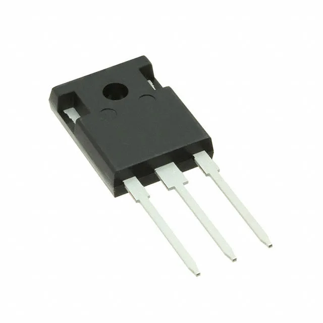
Infineon Technologies IPW60R190P6FKSA1

Infineon IPW60R190P6FKSA1 CoolMOS P6 N-Ch 600V 20.2A TO-247

MPNIPW60R190P6FKSA1
End of Life

Infineon CoolMOS™ P6, N-Channel MOSFET, 600 V Vdss, 20.2 A Id, 190 mOhm Rds(on) @ 7.6 A, 10 V, 11 nC Qg @ 10 V, TO-247-3 through hole, -55°C to 150°C TJ.

$3.6Ref. price · indicative, final on quote
PackagingTO-247-3
StockContact for availability
MOQ1 pcs
  • 100% new & originalTraceable channels only — no refurbs, no pulls, no remarked parts.
  • Date & lot codes on quoteStated per line before you commit; label photos on request.
  • MSL-compliant ESD packingMoisture-sealed bags with indicator cards; reels photo-verified.
  • PayPal buyer protectionPay by T/T, PayPal or Payoneer — card payments covered end to end.

Specifications

IPW60R190P6FKSA1 Technical Specifications
ParameterValue
SeriesCoolMOS™ P6
FET typeN-Channel
Mounting typeThrough Hole
Drain to source voltage600 V
Drive voltage (Max rds on, min rds on)10V
Current - continuous drain (Id) @ 25°C20.2A (Tc)
Power dissipation151W (Tc)
Operating temperature-55°C ~ 150°C (TJ)
PackageTube
Vgs±20V
TechnologyMOSFET (Metal Oxide)
CaseTO-247-3
Vgs(th) (Max) @ id4.5V @ 630µ
Rds on (Max) @ id, vgs190mOhm @ 7.6A, 10V
Gate charge (Qg) (Max) @ vgs11 nC @ 10 V
Input capacitance (Ciss) (Max) @ vds1750 pF @ 100 V

Product details

Conduction loss at the operating point

IPW60R190P6FKSA1 maximum on-resistance is 190 mOhm measured at 7.6 A drain current with 10 V gate drive. Total power dissipation is rated at 151 W at case temperature — the TO-247-3 package with its large tab can sink that into a heatsink, but the junction-to-case thermal path must be managed with proper mounting and thermal compound.

Temperature range and package rework

The through-hole TO-247-3 package (PG-TO247-3) is straightforward to hand-solder or wave-solder — no hot-air rework needed, just a decent iron and a clean pad. The large tab takes heat well, so preheat the board if the ground plane is heavy.

Frequently asked questions

What is the gate charge and why does it matter for switching?

The maximum gate charge is 11 nC at 10 V gate drive. This low Qg means the gate driver only needs a small current to charge the gate capacitance, enabling fast switching transitions and reducing switching losses in hard-switched topologies like PFC and LLC converters.

Can IPW60R190P6FKSA1 replace IPW60R190P6?

The suffix FKSA1 denotes the specific packaging and reel configuration (TO-247-3 in tube). Electrically the die is the same CoolMOS P6 600 V, 190 mOhm device. If your BOM calls for IPW60R190P6, confirm the package code matches — the FKSA1 variant is the through-hole TO-247 version.