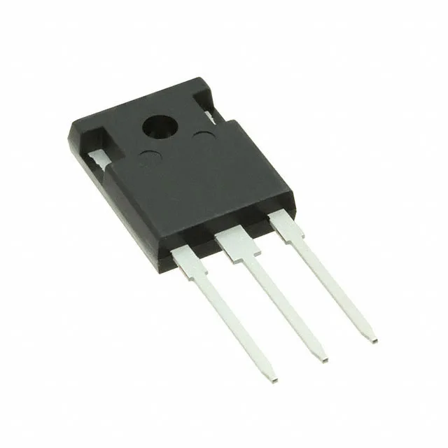
Infineon Technologies IPW60R125CFD7XKSA1

Infineon IPW60R125CFD7XKSA1 N-Channel MOSFET, 600 V, 18 A

MPNIPW60R125CFD7XKSA1
End of Life

Infineon OptiMOS IPW60R125CFD7XKSA1, N-channel MOSFET, 600 V drain-source, 125 mOhm Rds(on) at 10 V, 18 A continuous drain, TO-247-3 through-hole package, -55°C to 150°C junction temperature.

$5.3Ref. price · indicative, final on quote
PackagingTO-247-3
StockContact for availability
MOQ1 pcs
  • 100% new & originalTraceable channels only — no refurbs, no pulls, no remarked parts.
  • Date & lot codes on quoteStated per line before you commit; label photos on request.
  • MSL-compliant ESD packingMoisture-sealed bags with indicator cards; reels photo-verified.
  • PayPal buyer protectionPay by T/T, PayPal or Payoneer — card payments covered end to end.

Specifications

IPW60R125CFD7XKSA1 Technical Specifications
ParameterValue
SeriesOptiMOS™
FET typeN-Channel
Mounting typeThrough Hole
Drain to source voltage600 V
Drive voltage (Max rds on, min rds on)10V
Current - continuous drain (Id) @ 25°C18A (Tc)
Power dissipation92W (Tc)
Operating temperature-55°C ~ 150°C (TJ)
PackageTube
Vgs±20V
TechnologyMOSFET (Metal Oxide)
CaseTO-247-3
Vgs(th) (Max) @ id4.5V @ 390µA
Rds on (Max) @ id, vgs125mOhm @ 7.8A, 10V
Gate charge (Qg) (Max) @ vgs36 nC @ 10 V
Input capacitance (Ciss) (Max) @ vds1503 pF @ 400 V

Product details

600 V, 125 mOhm, 18 A — the hard-switching workhorse

The IPW60R125CFD7XKSA1: This is a hard-switching-optimised device from the OptiMOS CFD7 series, built for the primary side of switch-mode power supplies, PFC boost stages, and motor-drive inverters. The 600 V rating gives you 80 % derating margin on a 400 V DC bus, which is the standard headroom for flyback and half-bridge topologies.

Gate charge and switching loss — keep the driver honest

Total gate charge Qg is 36 nC at 10 V drive. Input capacitance Ciss is 1503 pF at 400 V drain-source, which sets the Miller plateau duration and the cross-conduction window in a half-bridge. Gate threshold voltage Vgs(th) is 4.5 V maximum at 390 µA drain current. That 4.5 V ceiling means a 10 V gate drive rail gives you a solid 5.5 V overdrive, pulling Rds(on) down to the rated 125 mOhm. Do not try to run this part on 5 V logic — the margin is too thin and conduction loss climbs fast.

Thermal and mechanical — TO-247 through-hole reality

Maximum power dissipation is 92 W at case temperature Tc. The TO-247-3 package with a copper tab lets you bolt the device to a heatsink — the junction-to-case thermal path is the limiting factor, not the silicon. Operating junction temperature covers -55°C to 150°C, so this part can sit in an engine bay or an outdoor telecom cabinet without a temperature-grade exception. Mounting is through-hole into the TO-247-3 footprint. The hole pattern and pad geometry are the same across the TO-247 family, so a board laid out for a 600 V CoolMOS sibling takes this part without a layout change.

Frequently asked questions

Is IPW60R125CFD7XKSA1 RoHS compliant?

Yes, the part is ROHS3 compliant per the Infineon product status. No RoHS exemption is needed for EU or UK market placement.