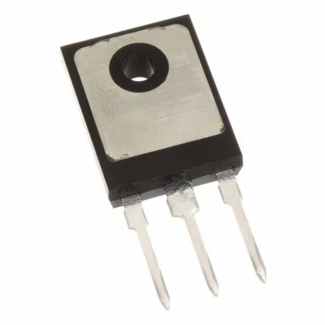
Infineon Technologies IPW60R045CPAFKSA1

Infineon IPW60R045CPAFKSA1 CoolMOS N-Ch MOSFET, 600 V, 60 A

MPNIPW60R045CPAFKSA1
End of Life

Infineon CoolMOS™ IPW60R045CPAFKSA1, N-Channel MOSFET, 600 V Vdss, 60 A Id, 45 mOhm Rds(on) @ 44 A, 10 V, PG-TO247-3, AEC-Q101, -40°C to 150°C.

$24.71Ref. price · indicative, final on quote
PackagingTO-247-3
StockContact for availability
MOQ1 pcs
  • 100% new & originalTraceable channels only — no refurbs, no pulls, no remarked parts.
  • Date & lot codes on quoteStated per line before you commit; label photos on request.
  • MSL-compliant ESD packingMoisture-sealed bags with indicator cards; reels photo-verified.
  • PayPal buyer protectionPay by T/T, PayPal or Payoneer — card payments covered end to end.

Specifications

IPW60R045CPAFKSA1 Technical Specifications
ParameterValue
SeriesCoolMOS™
FET typeN-Channel
Mounting typeThrough Hole
Drain to source voltage600 V
Drive voltage (Max rds on, min rds on)10V
Current - continuous drain (Id) @ 25°C60A (Tc)
Power dissipation431W (Tc)
Operating temperature-40°C ~ 150°C (TJ)
GradeAutomotive
PackageTube
Vgs±20V
TechnologyMOSFET (Metal Oxide)
QualificationAEC-Q101
CaseTO-247-3
Vgs(th) (Max) @ id3.5V @ 3mA
Rds on (Max) @ id, vgs45mOhm @ 44A, 10V
Gate charge (Qg) (Max) @ vgs190 nC @ 10 V
Input capacitance (Ciss) (Max) @ vds6800 pF @ 100 V

Product details

600 V CoolMOS with automotive-grade gate

The 45 mOhm typical on-resistance at 44 A and 10 V drive sets the conduction loss floor for high-efficiency switching stages. This part belongs to the CoolMOS family, Infineon's charge-compensation superjunction platform that delivers low Rds(on) per silicon area. The 190 nC total gate charge at 10 V Vgs gives the designer a concrete number for sizing the gate-drive supply and estimating switching losses at the target frequency.

On-resistance and switching charge

That 10 V drive voltage is the recommended rail for achieving the rated on-resistance; driving below 10 V leaves Rds(on) headroom on the table. Gate charge totals 190 nC at 10 V, with an input capacitance of 6800 pF at 100 V drain-source. The combination of moderate gate charge and low Rds(on) suits this part for hard-switching topologies like PFC boost stages and DC-DC converters in the 1 kW to 3 kW range.

Temperature envelope and power dissipation

Maximum power dissipation is 431 W at the case, but the real thermal limit depends on the heatsink and airflow — the junction-to-case thermal path is the constraint in a TO-247 package.

Active lifecycle and compliance

It is ROHS3 compliant, which clears the restriction-of-hazardous-substances gate for current-generation designs.

Frequently asked questions

Is IPW60R045CPAFKSA1 AEC-Q101 qualified?

Yes, the IPW60R045CPAFKSA1 is qualified to AEC-Q101, the automotive stress-test qualification for discrete semiconductors. This qualification covers the temperature range, reliability testing, and lot-traceability requirements for automotive and high-reliability industrial applications.

What is the Rds(on) of IPW60R045CPAFKSA1?

The maximum on-resistance is 45 mOhm at a drain current of 44 A with a 10 V gate-source drive. This is the figure to use for worst-case conduction loss calculations at the rated operating point.

What is the gate charge of IPW60R045CPAFKSA1?

Total gate charge is 190 nC at a 10 V gate drive. This value is used to calculate the gate-drive power: Pgate = Qg × Vgs × fsw. At 100 kHz switching, the gate-drive power is roughly 190 mW.

Is IPW60R045CPAFKSA1 RoHS compliant?

Yes, the part is ROHS3 compliant, meeting the current RoHS directive restrictions on lead, mercury, cadmium, and other substances.