150 V, 5.4 mOhm — the conduction-loss floor in a 48–72 V bus
This Rds(on) figure sets the conduction loss for a given load current — at 50 A the I²R loss is 13.5 W, which the PG-HDSOP-16-2 package can dissipate with a proper PCB copper area or heatsink. The 150 V Vdss provides headroom for 48 V and 72 V bus architectures common in telecom rectifiers, e-bike controllers, and industrial DC-DC converters, absorbing load-dump and switching transients without avalanche breakdown.
Total gate charge is 73 nC at 10 V, which determines the average gate-drive current at a given switching frequency. At 100 kHz the driver must supply 7.3 mA average; at 200 kHz that doubles to 14.6 mA. The input capacitance Ciss is 5700 pF at 75 V Vds, so the driver's peak current capability must charge this capacitance through the gate resistor within the desired turn-on time. The drive voltage range of 8 V to 10 V for minimum Rds(on) means a standard 10 V gate-drive rail is sufficient — no need for a 12 V boost regulator.
Thermal limits and the 175 °C junction ceiling
Power dissipation is rated at 3.8 W at 25 °C ambient (Ta) and 250 W at the case (Tc). The 143 A continuous drain current at case temperature is the package-limited figure — the practical board-level limit without a heatsink is the 17.5 A at 25 °C ambient. The wide Tj range also means the Rds(on) increase with temperature (typically 40–50 % higher at 125 °C) must be factored into the worst-case conduction loss budget.
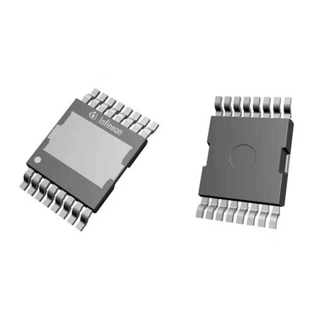
Package and mounting — PG-HDSOP-16-2 footprint
The large exposed drain pad on the bottom of the package provides the primary thermal path to the PCB.
It is ROHS3 compliant, meaning no restricted substances above the exemption thresholds.