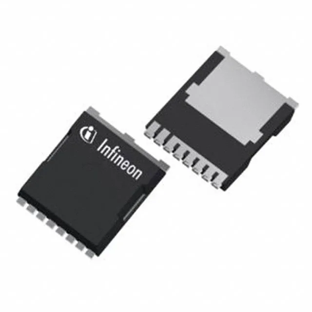
Infineon Technologies IPT60R150G7XTMA1

Infineon IPT60R150G7XTMA1 CoolMOS G7 N-Ch 650V 17A MOSFET

MPNIPT60R150G7XTMA1
End of Life

Infineon CoolMOS™ G7 series, N-Channel MOSFET, 650 V Drain-Source Voltage, 17 A Continuous Drain Current, 150 mOhm On-Resistance @ 10V, PG-HSOF-8-2 Package, -55°C to 150°C Operating Temperature.

$5.04Ref. price · indicative, final on quote
Packaging8-PowerSFN
StockContact for availability
MOQ1 pcs
  • 100% new & originalTraceable channels only — no refurbs, no pulls, no remarked parts.
  • Date & lot codes on quoteStated per line before you commit; label photos on request.
  • MSL-compliant ESD packingMoisture-sealed bags with indicator cards; reels photo-verified.
  • PayPal buyer protectionPay by T/T, PayPal or Payoneer — card payments covered end to end.

Specifications

IPT60R150G7XTMA1 Technical Specifications
ParameterValue
SeriesCoolMOS™ G7
FET typeN-Channel
Mounting typeSurface Mount
Drain to source voltage650 V
Drive voltage (Max rds on, min rds on)10V
Current - continuous drain (Id) @ 25°C17A (Tc)
Power dissipation106W (Tc)
Operating temperature-55°C ~ 150°C (TJ)
PackageTape & Reel (TR); Cut Tape (CT)
Vgs±20V
TechnologyMOSFET (Metal Oxide)
Case8-PowerSFN
Vgs(th) (Max) @ id4V @ 260µA
Rds on (Max) @ id, vgs150mOhm @ 5.3A, 10V
Gate charge (Qg) (Max) @ vgs23 nC @ 10 V
Input capacitance (Ciss) (Max) @ vds902 pF @ 400 V

Product details

The Infineon IPT60R150G7XTMA1 is a 650 V N-channel CoolMOS™ G7 MOSFET in a PG-HSOF-8-2 surface-mount package. It is a high-voltage switching device built for power conversion stages where low conduction and fast switching both matter. The 150 mOhm on-resistance at 5.3 A and 10 V increases with junction temperature. The PG-HSOF-8-2 exposed pad is the primary thermal path. The 23 nC total gate charge at 10 V keeps gate-drive energy low. A standard driver handles the load.

Switching and thermal — the parametric picture

Input capacitance is 902 pF at 400 V drain-source. That is a moderate figure — the driver sees a manageable capacitive load at turn-on, and the miller plateau stays short enough for clean edge rates in hard-switched topologies like PFC or LLC. The gate threshold voltage is 4 V maximum at 260 µA drain current. A 10 V gate drive is recommended for the rated Rds(on); the ±20 V Vgs absolute maximum allows margin. Power dissipation is rated at 106 W at the case. The PG-HSOF-8-2 exposed pad needs a good thermal via array and copper pour to keep the junction below 150°C at full load.

ROHS3 compliant — no exemptions for lead in solder or other restricted substances, which simplifies compliance for EU and global markets.

Package and footprint — what the PG-HSOF-8-2 needs

The 8-PowerSFN (PG-HSOF-8-2) is a surface-mount package with an exposed drain pad on the bottom. The pad is the primary thermal path and the drain connection — the PCB footprint must have a matching copper area and at least four thermal vias to the inner ground plane to get the 106 W dissipation rating. The package is compatible with standard reflow profiles.

Frequently asked questions

Can I swap this MOSFET on site with basic tools?

The PG-HSOF-8-2 is a surface-mount package with an exposed pad. Swapping it on site without a hot-air rework station or a temperature-controlled soldering iron with a large tip is risky — the pad needs uniform heat to reflow the solder underneath. Not a field-swap part unless you carry a hot-air station in the kit.