600 V CoolMOS G7 — switching loss and conduction floor
With a 34 nC total gate charge at 10 V, the gate drive power requirement at 100 kHz switching is about 34 mW, allowing standard gate drivers to handle the switching without excessive thermal stress.
Junction temperature and thermal budget
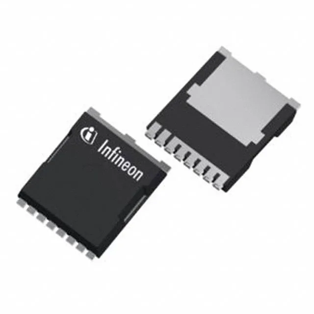
Maximum power dissipation is 141 W at case temperature, but the actual dissipation must be derated based on the junction-to-case thermal resistance and the heatsinking provided by the PCB copper area under the PG-HSOF-8-2 package. The 8-PowerSFN package (PG-HSOF-8-2) features an exposed drain pad that requires a thermal via pattern and adequate copper pour on the PCB to keep the junction temperature within the 150°C limit under full load.
Gate drive and switching characteristics
The gate threshold voltage is 4 V maximum at 390 µA drain current, meaning the device requires a gate drive above 4 V to begin conducting; the 10 V drive level is recommended to achieve the specified 102 mOhm Rds(on). Maximum gate-source voltage is ±20 V, so the gate drive circuit must be clamped to avoid exceeding this limit during switching transients or ringing. Input capacitance is 1320 pF maximum at 400 V drain-source, which together with the 34 nC gate charge defines the switching losses and the driver's peak current requirement.
Active production and compliance
The part is ROHS3 compliant, meeting the latest European Union restriction of hazardous substances directive for lead-free soldering processes.
Package and mounting
Surface-mount package in 8-PowerSFN (PG-HSOF-8-2) with an exposed drain pad for thermal management; the package is compatible with standard reflow soldering profiles.
