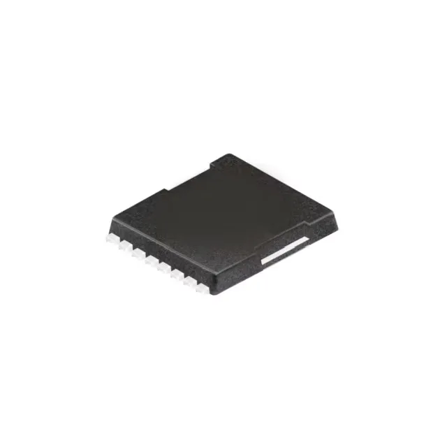
Infineon Technologies IPT030N12N3GATMA1 — Logic ICs

IPT030N12N3GATMA1 OptiMOS N-Ch 120V 3mOhm MOSFET, PG-HSOF-8

MPNIPT030N12N3GATMA1
End of Life

Infineon OptiMOS™ IPT030N12N3GATMA1, N-Channel MOSFET, 120 V, 3 mOhm max @ 100A, 237A Id, Surface Mount PG-HSOF-8, -55°C to 175°C.

$4.84Ref. price · indicative, final on quote
Packaging8-PowerSFN
StockContact for availability
MOQ1 pcs
  • 100% new & originalTraceable channels only — no refurbs, no pulls, no remarked parts.
  • Date & lot codes on quoteStated per line before you commit; label photos on request.
  • MSL-compliant ESD packingMoisture-sealed bags with indicator cards; reels photo-verified.
  • PayPal buyer protectionPay by T/T, PayPal or Payoneer — card payments covered end to end.

Specifications

IPT030N12N3GATMA1 Technical Specifications
ParameterValue
SeriesOptiMOS™
FET typeN-Channel
Mounting typeSurface Mount
Drain to source voltage120 V
Drive voltage (Max rds on, min rds on)10V
Current - continuous drain (Id) @ 25°C24A (Ta), 237A (Tc)
Power dissipation3.8W (Ta), 375W (Tc)
Operating temperature-55°C ~ 175°C (TJ)
PackageTape & Reel (TR); Cut Tape (CT)
Vgs±20V
TechnologyMOSFET (Metal Oxide)
Case8-PowerSFN
Vgs(th) (Max) @ id4V @ 270µA
Rds on (Max) @ id, vgs3mOhm @ 100A, 10V
Gate charge (Qg) (Max) @ vgs198 nC @ 10 V
Input capacitance (Ciss) (Max) @ vds13000 pF @ 60 V

Product details

3 mOhm Rds(on) — conduction loss floor for high-current rails

That Rds(on) figure is the part's defining spec: in a 100 A continuous load, conduction loss sits at roughly 30 W before factoring in temperature derating.

Gate charge and driver budget

Gate charge is 198 nC at 10 V, with an input capacitance of 13000 pF at 60 V Vds. That Qg number sets the gate-driver peak current requirement: switching at 100 kHz with a 10 V drive swing, the average gate current is roughly 0.2 A, but the peak during the Miller plateau can exceed 2 A if the driver is sized for fast edges. A standard 1 A gate-driver IC will work at moderate frequencies; for hard-switching above 200 kHz, plan on a driver with 4 A or more peak capability to avoid excessive switching loss.

Package and thermal path

The PG-HSOF-8 (8-PowerSFN) surface-mount package uses a large exposed drain pad. Thermal resistance is split between the junction-to-ambient (3.8 W Ta) and junction-to-case (375 W Tc) ratings — the case figure is the one that matters when the pad is soldered to a copper plane. The package is MSL 3; bake before reflow if the moisture-barrier bag has been open longer than the floor-life window.

Frequently asked questions

What is the difference between IPT030N12N3GATMA1 and IPT020N12N3G?

The IPT020N12N3G is a lower-Rds(on) variant in the same 120 V OptiMOS™ family. The IPT030N12N3GATMA1 has a 3 mOhm maximum Rds(on) at 100 A; the IPT020N12N3G is specified at 2 mOhm. The trade-off is cost and slightly higher gate charge for the lower-resistance part. Both share the same PG-HSOF-8 footprint and 175°C junction rating.