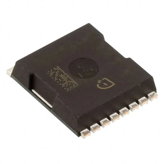
Infineon Technologies IPT015N10N5ATMA1

Infineon IPT015N10N5ATMA1 OptiMOS N-Ch 100V 300A MOSFET

MPNIPT015N10N5ATMA1
End of Life

Infineon OptiMOS series, IPT015N10N5ATMA1, N-Channel MOSFET, 100 V Vdss, 300 A Id, 1.5 mOhm Rds(on) at 150 A, 10 V, 211 nC Qg, PG-HSOF-8-1 package, -55°C to 175°C junction.

$6.85Ref. price · indicative, final on quote
Packaging8-PowerSFN
StockContact for availability
MOQ1 pcs
  • 100% new & originalTraceable channels only — no refurbs, no pulls, no remarked parts.
  • Date & lot codes on quoteStated per line before you commit; label photos on request.
  • MSL-compliant ESD packingMoisture-sealed bags with indicator cards; reels photo-verified.
  • PayPal buyer protectionPay by T/T, PayPal or Payoneer — card payments covered end to end.

Specifications

IPT015N10N5ATMA1 Technical Specifications
ParameterValue
SeriesOptiMOS™
FET typeN-Channel
Mounting typeSurface Mount
Drain to source voltage100 V
Drive voltage (Max rds on, min rds on)6V, 10V
Current - continuous drain (Id) @ 25°C300A (Tc)
Power dissipation375W (Tc)
Operating temperature-55°C ~ 175°C (TJ)
PackageTape & Reel (TR); Cut Tape (CT)
Vgs±20V
TechnologyMOSFET (Metal Oxide)
Case8-PowerSFN
Vgs(th) (Max) @ id3.8V @ 250µA
Rds on (Max) @ id, vgs1.5mOhm @ 150A, 10V
Gate charge (Qg) (Max) @ vgs211 nC @ 10 V
Input capacitance (Ciss) (Max) @ vds16000 pF @ 50 V

Product details

100 V, 300 A N-channel — the conduction-loss floor

The Infineon IPT015N10N5ATMA1 is an OptiMOS N-channel power MOSFET rated for 100 V drain-source and 300 A continuous drain current at a 25°C case temperature.

Gate charge and the driver it needs

Total gate charge is 211 nC at 10 V. That is not a trivial load — a gate driver must source several amperes peak to switch this FET in the tens of nanoseconds. If your driver is marginal on peak current, the switching edges slow, and the device spends more time in the linear region, which burns the thermal margin you thought you had from the 1.5 mOhm Rds(on). The input capacitance is 16000 pF at 50 V Vds. That capacitance, together with the gate charge, determines the drive power at frequency. At 100 kHz switching, the gate-drive loss alone is about 0.2 W — manageable, but it adds to the total dissipation in the driver IC.

175°C junction — where it lives

That 175°C ceiling qualifies it for under-hood automotive and industrial environments. The 375 W power dissipation at case temperature is a package limit.

Listed as Active in production.

PG-HSOF-8-1 — what the footprint needs

Surface-mount in an 8-PowerSFN package, supplier device package PG-HSOF-8-1. The gate drive voltage is specified at 6 V minimum for the rated Rds(on); 10 V is the standard drive level for the 1.5 mOhm figure.

Frequently asked questions

Is IPT015N10N5ATMA1 RoHS compliant?

Yes, it is listed as ROHS3 Compliant, meeting the latest EU RoHS directive requirements.

What is the recommended PCB layout for IPT015N10N5ATMA1?

Use multiple thermal vias under the pad to conduct heat to inner layers. The gate drive trace should be kept short and wide to minimize inductance; place the gate-driver IC as close as possible to the FET. Follow Infineon's application note for the OptiMOS 5 power stage layout guidelines.