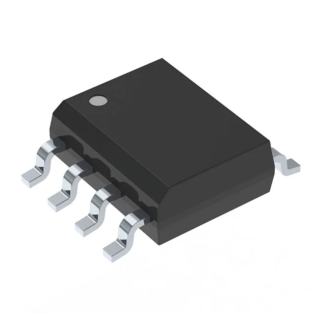
It switches a load supply from 6 V to 28 V, delivering up to 1.6 A continuous output with a typical on-resistance of 110 mOhm.
110 mOhm Rds(on) and 1.6 A — sizing the load budget
The 110 mOhm typical on-resistance at 25°C sets the conduction loss floor: at 1.6 A the I²R loss is about 280 mW, which the SOIC-8 package can dissipate with adequate copper on the PCB. Derate for ambient temperature above 25°C — the junction-to-ambient thermal resistance of the SOIC-8 without a heatsink pad is roughly 120°C/W, so the die temperature rise at full current is around 34°C above the board temperature. The 1.6 A maximum output rating is the absolute ceiling — real designs should budget 20% headroom below that for reliable operation over temperature and load transients. A load drawing 1.2 A continuous is a comfortable fit.
Non-inverting input and high-side topology
The high-side output configuration places the switch between the positive supply rail and the load, which is the typical arrangement for grounded-load switching in automotive and industrial systems.
Package and footprint — 8-SOIC narrow body
The footprint is standard — any SOIC-8 land pattern works, but confirm the body width matches your solder paste stencil aperture.