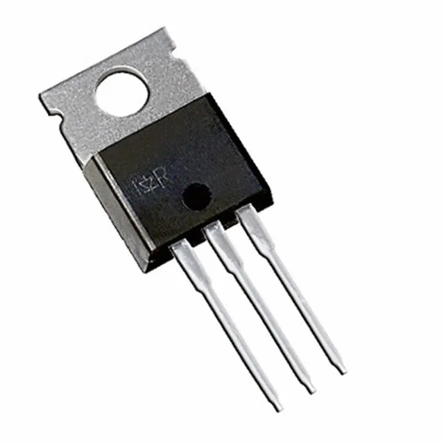
900 V CoolMOS — the high-voltage PFC and flyback switch
At 150°C junction temperature, the on-resistance roughly doubles from the 25°C value — a standard silicon MOSFET characteristic — so a 5 A load at high ambient may dissipate 17 W, not 8.5 W. The 94 nC total gate charge at 10 V means a gate driver delivering 1 A can switch the FET in about 94 ns; a 0.5 A driver takes 188 ns. Input capacitance is 2400 pF at 100 V drain-source, which loads the driver's output stage and sets the crossover time in a half-bridge leg.
Through-hole package and thermal interface
That figure assumes the tab is bolted to an infinite heatsink — in practice, the junction-to-case thermal resistance (not listed here) and the heatsink's own Rth determine the real limit. The through-hole mounting is preferred in designs where the PCB copper alone cannot sink the heat, such as in a 150 W PFC boost stage or a flyback converter with a 100 V output rail.
It is ROHS3 compliant.