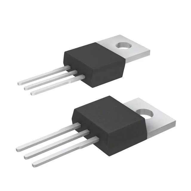
Infineon Technologies IPP65R110CFDXKSA2

Infineon IPP65R110CFDXKSA2 CoolMOS CFD2 N-Ch 650V 31.2A

MPNIPP65R110CFDXKSA2
End of Life

Infineon CoolMOS™ CFD2, N-Channel MOSFET, 650 V Vdss, 31.2 A Id, 110 mOhm Rds(on) @ 12.7 A, 10 V, 118 nC Qg, TO-220-3, Through Hole, -55°C to 150°C.

$6.25Ref. price · indicative, final on quote
PackagingTO-220-3
StockContact for availability
MOQ1 pcs
  • 100% new & originalTraceable channels only — no refurbs, no pulls, no remarked parts.
  • Date & lot codes on quoteStated per line before you commit; label photos on request.
  • MSL-compliant ESD packingMoisture-sealed bags with indicator cards; reels photo-verified.
  • PayPal buyer protectionPay by T/T, PayPal or Payoneer — card payments covered end to end.

Specifications

IPP65R110CFDXKSA2 Technical Specifications
ParameterValue
SeriesCoolMOS™ CFD2
FET typeN-Channel
Mounting typeThrough Hole
Drain to source voltage650 V
Drive voltage (Max rds on, min rds on)10V
Current - continuous drain (Id) @ 25°C31.2A (Tc)
Power dissipation277.8W (Tc)
Operating temperature-55°C ~ 150°C (TJ)
PackageTube
Vgs±20V
TechnologyMOSFET (Metal Oxide)
CaseTO-220-3
Vgs(th) (Max) @ id4.5V @ 1.3mA
Rds on (Max) @ id, vgs110mOhm @ 12.7A, 10V
Gate charge (Qg) (Max) @ vgs118 nC @ 10 V
Input capacitance (Ciss) (Max) @ vds3240 pF @ 100 V

Product details

650 V switching in a TO-220 — the CoolMOS CFD2 choice

The IPP65R110CFDXKSA2 is rated at 650 V Vdss, suitable for power factor correction stages, flyback converters, and LLC resonant topologies in industrial and telecom power supplies.

110 mOhm Rds(on) — conduction loss anchor

At 31.2 A full load, conduction loss at 110 mOhm (ignoring temperature derating) is roughly 107 W; the 277.8 W maximum power dissipation in the TO-220 package gives thermal headroom for a properly heatsinked design, but the actual junction temperature rise must be calculated against the operating current and switching losses.

Gate charge and switching speed

Total gate charge is 118 nC at 10 V gate drive, with an input capacitance of 3240 pF at 100 V drain-source — these numbers set the switching driver requirement and the transition loss budget. A gate driver capable of sourcing and sinking a few amperes peak is needed to charge and discharge 118 nC within the target dead-time; the ±20 V maximum gate-source rating accommodates standard gate drive levels with margin.

Frequently asked questions

Can I use the IPP65R110CFDXKSA2 in a 400V DC bus application?

Yes. The 650 V drain-source rating provides 250 V of headroom above a 400 V DC bus, which is typical for power factor correction and flyback stages. The margin covers switching overshoot and line transients.